

What Makes PCB Via Design Reliable for High-Speed Boards?
- Posted On:
- November 10, 2026
- Category:
- Ecad

A high-speed PCB can have controlled-impedance traces, a planned stackup, and clean routing yet still develop signal-integrity problems at a layer transition.
The via may be the missing piece.
In interfaces such as PCIe, DDR5, USB 3.x, and high-speed SerDes, a via is more than a connection between copper layers. Its stub length, pad geometry, antipad, reference planes, and return path all influence signal behavior.
Reliable PCB via design keeps the vertical transition electrically predictable.
Why PCB Via Design Matter in High-Speed Design
A via changes the electrical environment around a high-speed signal.
Its barrel, pad, antipad, surrounding copper, and dielectric material introduce parasitic inductance and capacitance. These can create impedance discontinuities, causing signal reflections and degrading signal quality.
Fast edge rates make these effects more significant, even when the clock frequency itself is moderate.
High-speed vias can therefore affect:
- Signal reflections
- Insertion and return loss
- Eye-diagram quality
- Crosstalk
- EMI
- Timing margin
A reliable via keeps the signal and return paths predictable through the layer transition.
What Makes a High-Speed Via Reliable?
1. Control the Via Stub Length
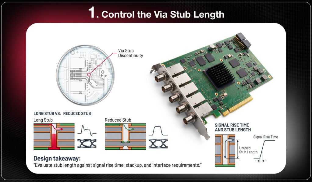
A via stub is the unused portion of a plated via barrel extending beyond the layer where the signal exits.
Although it is not part of the intended connection, the remaining barrel still affects the signal electrically.
Long stubs can introduce:
- Reflections
- Resonance
- Impedance discontinuities
- Eye-diagram degradation
As a practical example, a 1 mm stub can produce a quarter-wave resonance in the tens-of-GHz range, depending on the effective dielectric constant and via structure.
Back drilling removes unused barrel length, while blind or buried vias can avoid unnecessary stubs.
Design takeaway: Evaluate stub length against signal rise time, stackup, and interface requirements.
2. Maintain a Continuous Return-Current Path
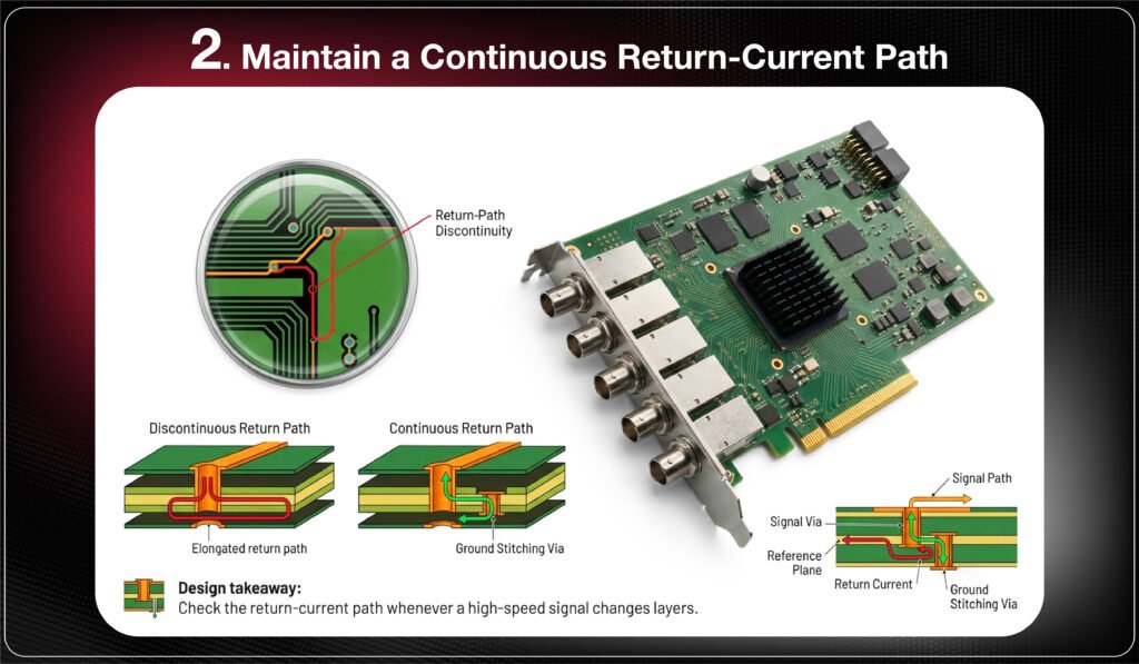
A high-speed signal needs a return-current path, typically through a nearby reference plane.
When a signal changes layers and its reference plane becomes discontinuous, return current may be forced to take a longer path.
This increases loop inductance and can worsen:
- EMI
- Crosstalk
- Signal integrity
- Ground noise
Ground stitching vias can help maintain a lower-impedance return path between reference planes near critical transitions.
Design takeaway: Check the return-current path whenever a high-speed signal changes layers.
3. Optimize Pad and Antipad Geometry
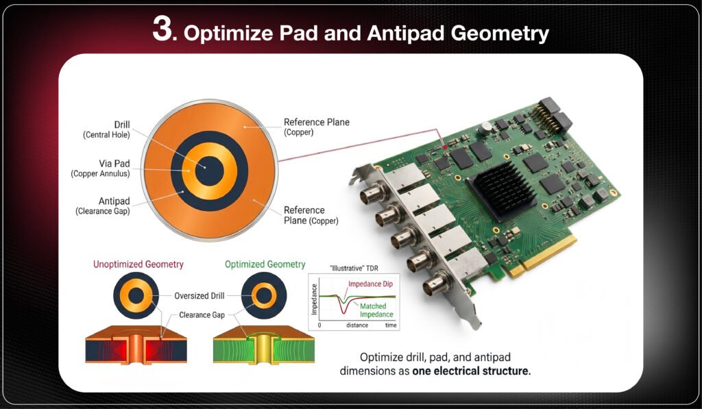
Via geometry directly affects its electrical characteristics.
The antipad is the clearance opening around a via in a copper plane. Drill diameter, pad diameter, antipad size, dielectric thickness, and plane spacing work together to determine the transition’s parasitic behavior.
Increasing the antipad can reduce capacitive loading, while excessive clearance can affect routing density and plane continuity. Smaller vias may improve electrical performance but introduce fabrication challenges.
Design takeaway: Optimize drill, pad, and antipad dimensions as one electrical structure.
4. Keep Differential Via Transitions Symmetrical
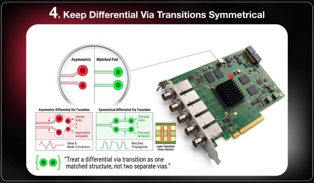
Interfaces such as PCIe, USB 3.x, and SerDes require differential signals to experience closely matched electrical environments.
Even when a differential pair is correctly routed, an asymmetric via transition can introduce:
- Differential skew
- Mode conversion
- Common-mode noise
- Reduced eye opening
For better performance:
- Keep both vias geometrically consistent.
- Maintain pair spacing.
- Preserve the reference-plane relationship.
- Avoid unnecessary asymmetry.
Design takeaway: Treat a differential via transition as one matched structure, not two separate vias.
5. Validate Critical Via Structures with SI Analysis
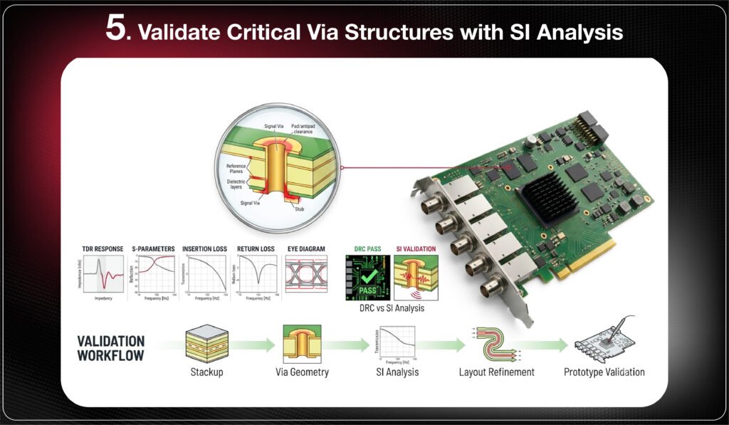
Passing DRC does not guarantee high-speed electrical performance.
DRC verifies physical design rules but does not fully evaluate the three-dimensional electromagnetic behavior of a critical via.
For demanding interfaces, engineers may evaluate:
- TDR response
- S-parameters
- Insertion loss
- Return loss
- Eye diagrams
A practical validation flow is:
Stackup → Via geometry → SI analysis → Layout refinement → Prototype validation
Design takeaway: Validate critical transitions against actual interface requirements, not only DRC.
Choosing the Right Via Structure
The correct via structure depends on electrical requirements, stackup, fabrication capability, routing density, and cost.
A through via is simple and economical when its remaining stub is acceptable.
A blind via connects selected layers without passing through the entire board, reducing unnecessary barrel length.
A back-drilled via removes the unused portion of a through-hole barrel and is useful when a long stub affects signal integrity.
Consider:
- Signal rise time
- Stub length
- Stackup
- Layer transition requirements
- Routing density
- Fabrication capability
- Cost
The most advanced via technology is not automatically the best solution.
Common High-Speed Via Design Problems
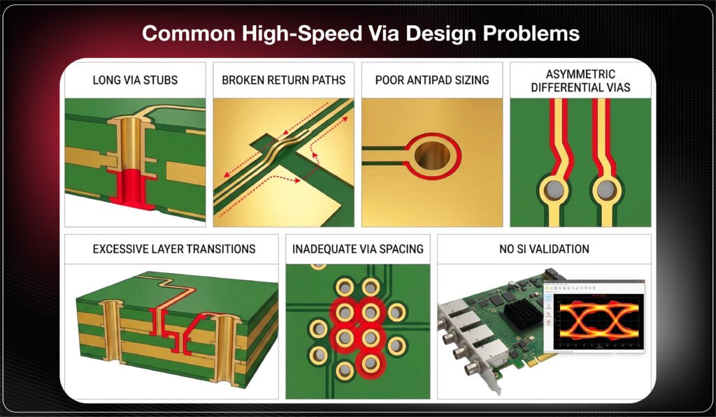
Common issues include:
- Long via stubs
- Broken return paths
- Poor antipad sizing
- Asymmetric differential vias
- Excessive layer transitions
- Inadequate via spacing
- No SI validation
These can cause data errors, timing-margin loss, EMI, and degraded link performance
Real-World Engineering Insight
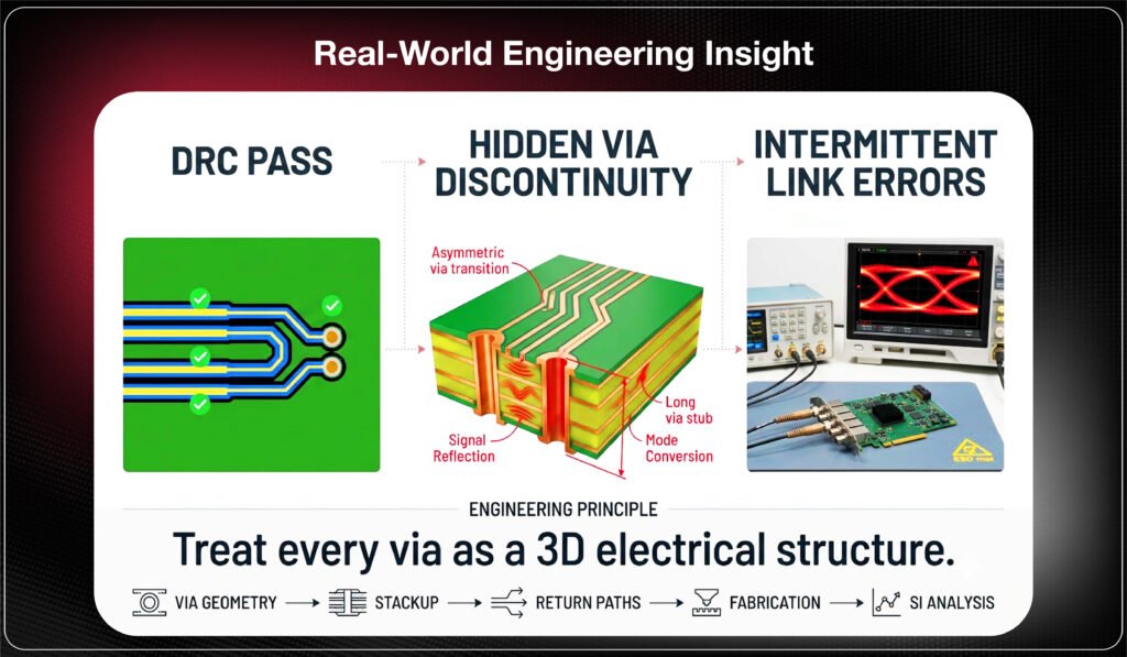
A high-speed differential link may pass DRC and look correct during layout review but develop intermittent errors during hardware validation.
An asymmetric via transition or long stub can introduce reflection and mode conversion, reducing the receiver’s voltage and timing margin.
This is why a via should be treated as a 3D electrical structure, not simply a 2D layout feature.
Reliable design connects via geometry, stackup, return paths, fabrication, and SI analysis before prototype validation.
Final Answer
Choose a standard enclosure design when an existing housing meets the product’s requirements without major compromises.
Choose custom enclosure design when the product needs specific dimensions, connector locations, thermal solutions, protection, mounting, or industrial-design features.
The decision should begin with the product requirements, not the enclosure catalog.
The right enclosure is not simply the one that fits the PCB; it is the one that supports the complete product.
Improve product fit and reliability.
Start enclosure design early.
Book a Call. Schedule a Free Consultation now. https://calendly.com/gighz/30min
Frequently Asked Questions
- Why are vias important in high-speed PCB design?
Vias can introduce parasitic, impedance discontinuities, and signal reflections. - What is a via stub?
An unused barrel section that can cause reflections and resonance. - When is back drilling needed?
When a via stub becomes electrically significant to the signal. - Why is the return path important?
An interrupted return path can increase EMI, crosstalk, and signal-integrity issues. - Does DRC guarantee reliable vias?
No. Critical vias may require SI analysis to verify electrical performance.
Stuck in a loop of challenges? Always pick smart solution that works
Have you faced costly rework because 2D drawings skipped in MCAD workflows?
Effective way to prevent MCAD documentation errors recalls?
Please answer both poll questions before submitting.
Thank you for your response! 😊
Latest Post
Get Customized Engineering CAD Design Service

Book a Free Consultation Call
Partner with Gighz and bring your most innovative design concepts to life. Our engineering cad services accelerate development so you can focus on your big vision.
