


Many engineers assume PCB costs mainly depends on board size, layer count, and component prices. While these factors matter, they are only part of the equation.
A PCB can look simple on paper but become expensive because of decisions made during design.
Poor stack-up planning, inefficient component placement, unnecessary routing complexity, signal integrity issues, and manufacturing challenges can increase fabrication costs and even lead to costly redesigns.
The biggest PCB expenses are often not caused by manufacturing—they are caused by design choices made before the board reaches the factory.
Understanding these hidden cost drivers helps engineers create boards that are reliable, easier to manufacture, and more cost-effective.
What Really Drives PCB Costs?
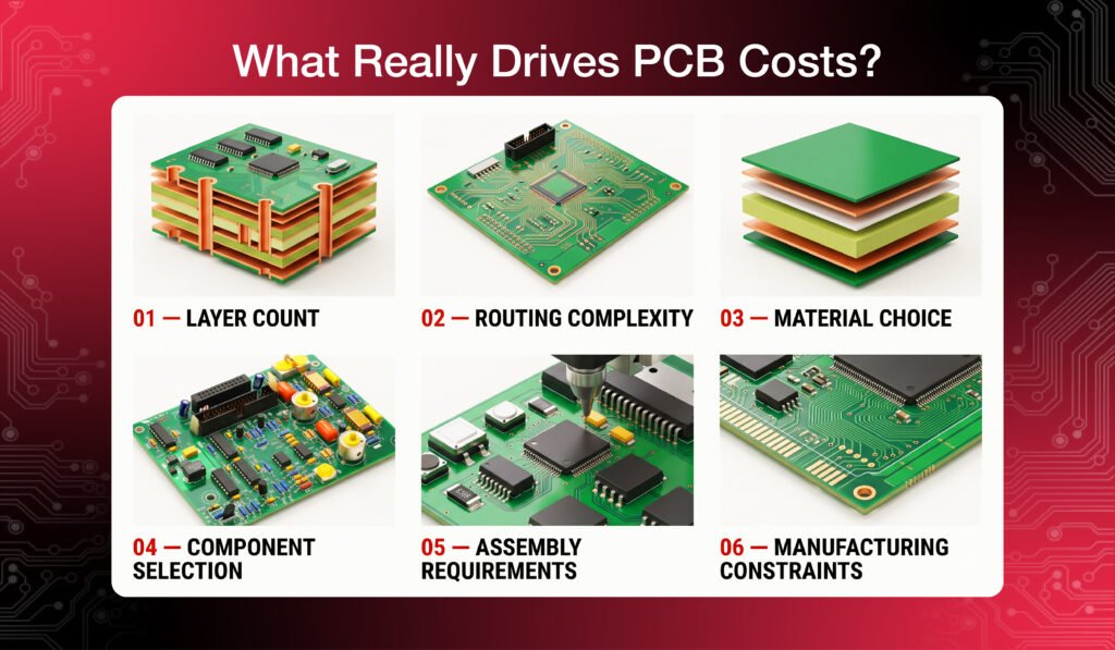
The final price of a PCB depends on several design decisions, not just the board itself.
Factors such as layer count, routing complexity, material choice, component selection, assembly requirements, and manufacturing constraints all influence the overall cost.
For example, adding extra layers may simplify routing but increase fabrication expenses, while premium materials may add cost without improving the design.
The key is finding the right balance between performance, reliability, and manufacturability. Let’s look at the design choices that quietly increase expenses.
1. Poor PCB Stack-up Planning
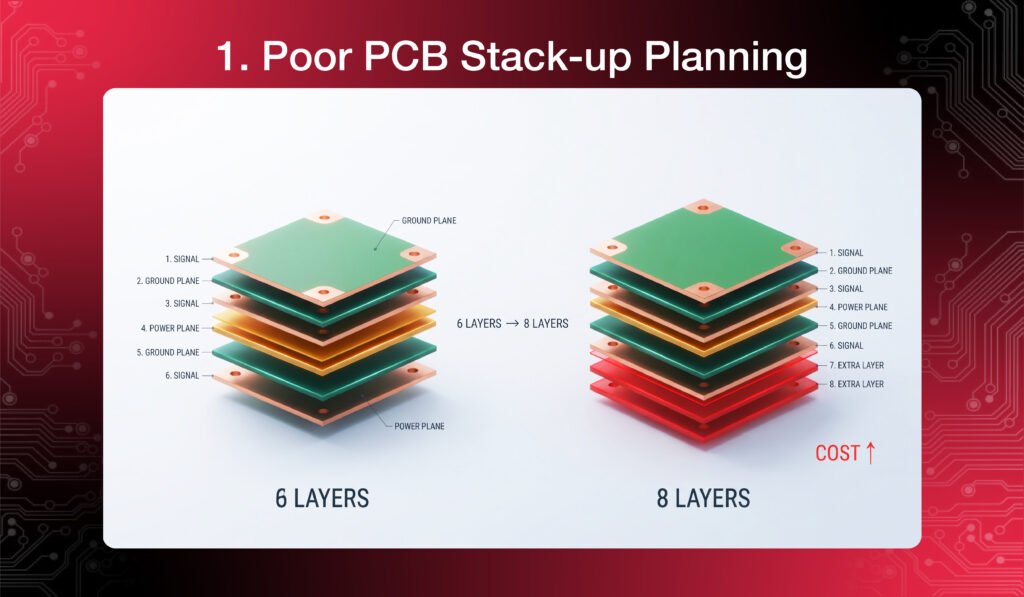
The PCB layer stack-up is one of the first decisions that impacts cost.
Adding more layers provides additional routing space and improves signal integrity, but every extra layer increase manufacturing complexity. More layers require additional copper, prepreg materials, lamination cycles, drilling processes, and inspection.
For example, a design that can be completed with six layers may unnecessarily use eight layers because of poor planning. That additional complexity directly increases the manufacturing cost.
A properly planned stack-up considers:
- Signal routing requirements
- Power and ground planes
- Impedance control
- Manufacturing capability
Choosing the right number of layers from the beginning prevents unnecessary expenses.
2. Incorrect Component Placement
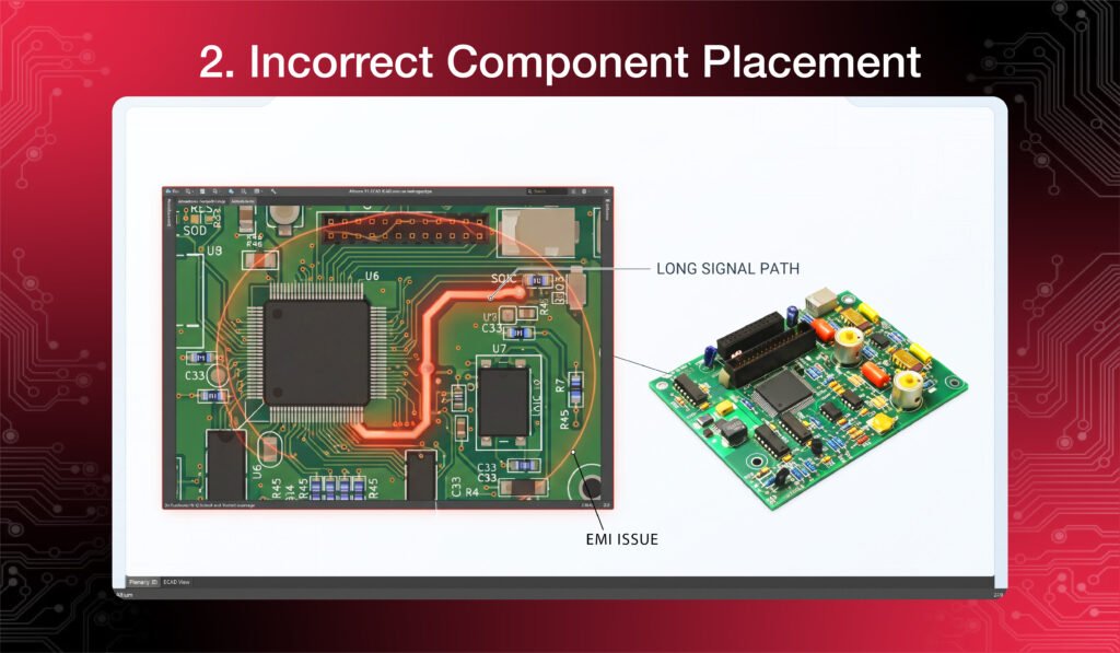
Component placement affects routing effort, signal performance, and assembly cost.
When related components are placed far apart, traces become longer and require more vias and layer changes. Poor placement can also create EMI issues, thermal problems, and difficult assembly conditions.
For high-speed designs, placement becomes even more critical. Memory devices, processors, and power components must be positioned carefully to maintain short and controlled signal paths.
A good placement strategy reduces routing complexity and improves overall PCB reliability.
3. Overly Complex Routing

Routing is not just about connecting components—it directly affects the cost and performance.
Unnecessary routing complexity often comes from:
- Excessive vias
- Too many layers transitions
- Long trace paths
- Unnecessary meandering traces
Every additional via increases manufacturing steps, while complex routing makes the board harder to manufacture and debug.
Efficient routing focuses on keeping critical signals short, maintaining proper return paths, and avoiding unnecessary complexity.
4. Ignoring Signal Integrity Early
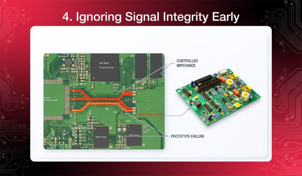
Signal integrity problems are expensive when discovered late.
High-speed interfaces such as DDR5, PCIe, USB4, Ethernet, and SERDES require careful planning for:
- Controlled impedance
- Differential pair routing
- Return current paths
- Length matching
- Crosstalk reduction
If these requirements are ignored during the initial design stage, engineers may discover failures during prototype testing. Fixing these issues often requires major layout changes or another PCB revision.
Planning signal integrity from the beginning saves both time and development cost.
5. Poor Power Distribution Design
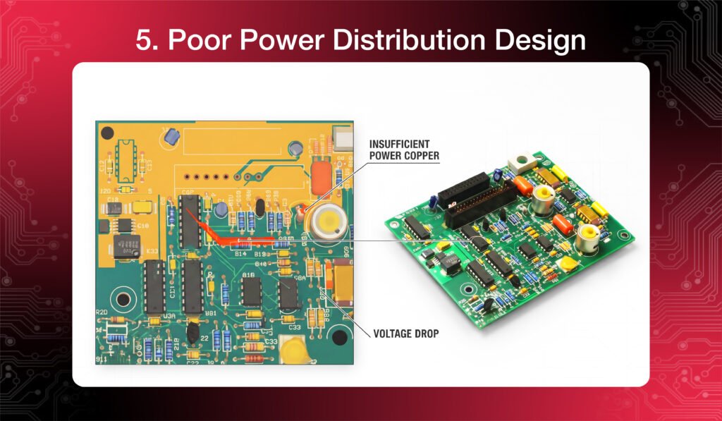
Power delivery problems are another hidden cause of PCB redesigns.
Insufficient copper width, poor ground connections, and weak power planes can create:
- Voltage drops
- Power noise
- Thermal issues
- Unstable operation
Fixing these problems after fabrication may require thicker copper, additional layers, or complete layout changes.
A properly designed Power Distribution Network (PDN) ensures stable operation and avoids expensive modifications later.
6. Unnecessary High-Speed Design Rules
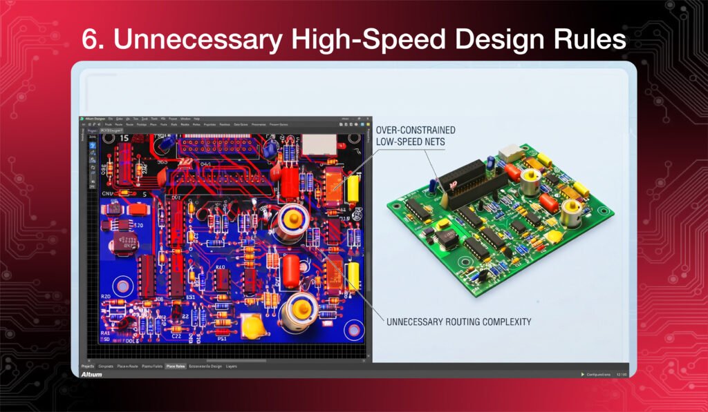
Not every signal requires advanced routing rules.
Controlled impedance, matched lengths, and strict spacing requirements are essential for high-speed interfaces, but applying these rules to every net increase design complexity and development time.
Signals such as simple GPIO, LEDs, and basic control lines usually do not require the same level of constraint.
Using high-speed rules only where needed helps reduce unnecessary cost and effort.
7. Choosing the Wrong PCB Material
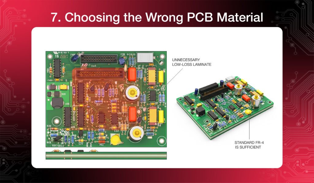
Material selection should depend on application requirements.
Standard FR-4 is suitable for most electronic designs. However, some projects use expensive low-loss laminates without a real technical requirement.
Specialized materials are necessary for RF applications, microwave circuits, and extremely high-speed designs. But using them unnecessarily increases cost without improving performance.
The right material is the one that meets the design requirements—not the most expensive option.
8. Ignoring Design for Manufacturability (DFM)
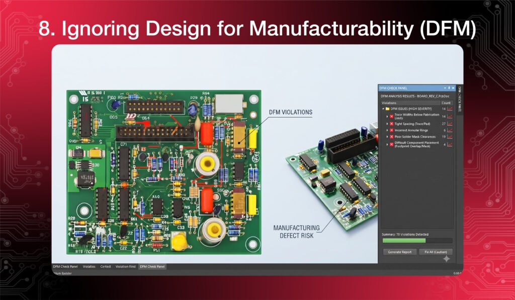
A PCB that works in design software may still face manufacturing problems.
Common DFM issues include:
- Trace widths below fabrication limits
- Tight spacing
- Incorrect annular rings
- Poor solder mask clearances
- Difficult component placement
These problems can cause fabrication delays, assembly defects, and additional costs.
Performing DFM checks before manufacturing helps identify problems early and improves first-pass success.
9. Skipping Design Reviews
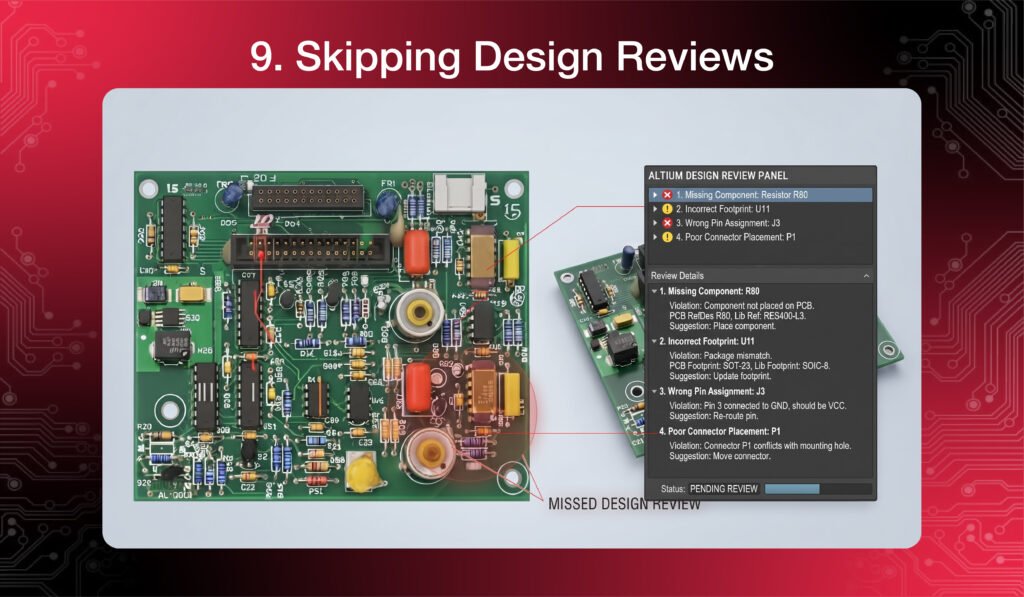
A detailed design review is one of the easiest ways to prevent unnecessary PCB expenses.
Reviews can identify issues such as:
- Incorrect footprints
- Missing components
- Wrong pin assignments
- Poor connector placement
- Manufacturing concerns
Finding these mistakes before fabrication is inexpensive. Finding them after prototypes are built can cost weeks of engineering time and additional production expenses.
Final Thought
PCB costs are not determined only by board size or component count. Design decisions made during schematic creation and PCB layout have a major impact on manufacturing cost, reliability, and development time.
By planning the stack-up carefully, optimizing placement, simplifying routing, considering signal integrity, and following manufacturing guidelines, engineers can create better-performing PCBs without unnecessary expenses.
A cost-effective PCB is not the cheapest board—it is the one designed correctly from the start.
Improve PCB performance and reliability.
Partner with us for PCB solutions.
Want to avoid hidden issues in your design?
Connect with us for the expert free consultation
https://calendly.com/gighz/30min
Stuck in a loop of challenges? Always pick smart solution that works
Have you faced costly rework because 2D drawings skipped in MCAD workflows?
Effective way to prevent MCAD documentation errors recalls?
Please answer both poll questions before submitting.
Thank you for your response! 😊
Latest Post
Get Customized Engineering CAD Design Service

Book a Free Consultation Call
Partner with Gighz and bring your most innovative design concepts to life. Our engineering cad services accelerate development so you can focus on your big vision.
