

15 PCB Layer Stackup Mistakes Every Hardware Team Should Fix
- Posted On:
- October 14, 2026
- Category:
- Ecad

The Most Expensive PCB Mistakes Can Start Before Routing
Before routing begins, your PCB stackup has already shaped its electrical and mechanical performance.
Layer count, plane placement, dielectric thickness, copper weight, and materials all influence impedance, EMI, power delivery, thermal behavior, warpage, and manufacturing cost.
A poorly planned stackup can create failures that appear only during testing or production—when fixes are expensive.
That is why stackup planning deserves the same attention as schematic design and routing.
Here are 15 common PCB layer stackup mistakes every hardware team should identify before they become costly problems.
Why Layer Stackup Matters for Reliable Hardware Design
A PCB layer arrangement defines how copper and dielectric layers are positioned inside the board. It directly affects electrical performance, mechanical stability, and fabrication success.
A well-planned stackup helps:
- Maintain controlled impedance
- Improve signal integrity
- Provide stable power distribution
- Reduce EMI problems
- Improve manufacturing yield
- Prevent costly redesigns
Many stackup-related failures happen because decisions are made too late in the design process. Let’s look at the common mistake’s hardware teams should avoid.
15 Common PCB Layer Stackup Mistakes to Avoid
1. Starting PCB Layout Before Finalizing the Stackup
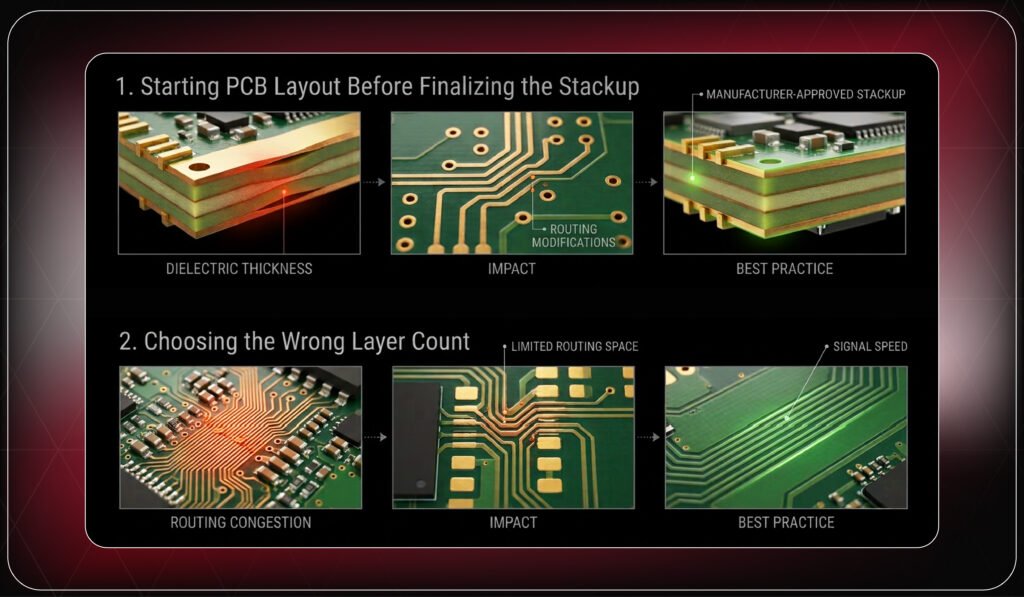
Beginning routing before confirming the layer structure often leads to major changes later when dielectric thickness, copper weight, or material selection changes.
Impact:
- Routing modifications
- Project delays
- Additional engineering effort
Best practice:
Finalize the manufacturer-approved stackup before component placement and routing begin.
2. Choosing the Wrong Layer Count
Too few layers create routing congestion, while unnecessary layers increase fabrication costs.
Impact:
- Limited routing space
- Poor power distribution
- Higher production cost
Best practice:
Select layer count based on routing density, signal speed, power requirements, and manufacturing capability.
3. Ignoring Manufacturer Stackup Recommendations
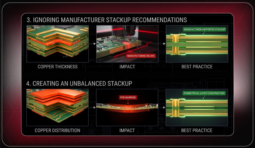
PCB manufacturers have specific capabilities for materials, copper thickness, dielectric spacing, and fabrication processes.
Impact:
- Manufacturing delays
- Stackup redesign
- DFM issues
Best practice:
Use manufacturer-supported stackup configurations whenever possible.
4. Creating an Unbalanced Stackup
Uneven copper distribution creates mechanical stress during lamination.
Impact:
- PCB warpage
- Layer deformation
- Lower production yield
Best practice:
Maintain symmetrical layer construction and balanced copper distribution.
5. Poor Ground Plane Placement
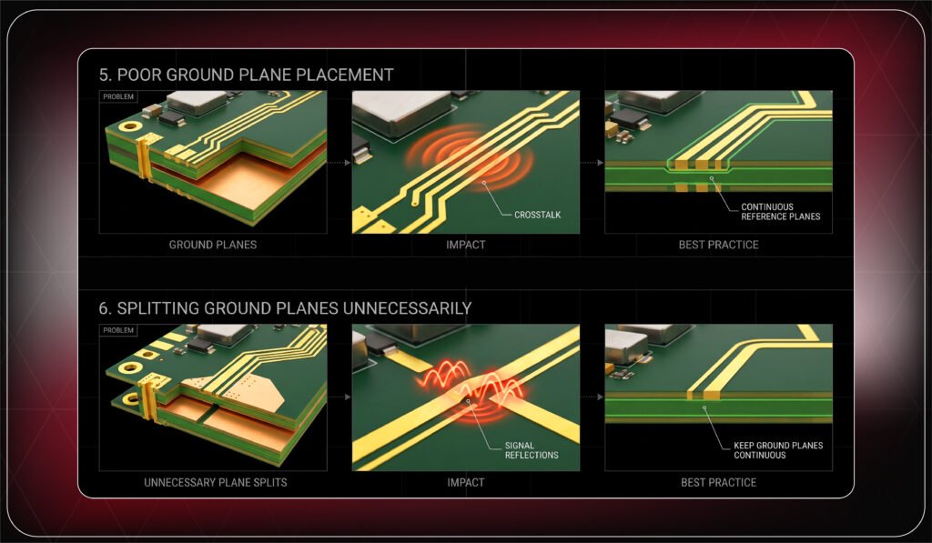
Ground planes provide return paths for high-speed signals. Poor placement increases noise and EMI risk.
Impact:
- Crosstalk
- Signal integrity issues
- EMI failures
Best practice:
Place continuous reference planes close to critical signal layers.
6. Splitting Ground Planes Unnecessarily
Unnecessary plane splits interrupt return current paths and create unwanted noise.
Impact:
- Signal reflections
- Increased interference
- EMC problems
Best practice:
Keep ground planes continuous unless isolation is required.
7. Ignoring Controlled Impedance Requirements
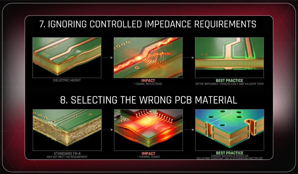
Impedance is determined by trace width, copper thickness, dielectric height, and material properties—not routing alone.
Impact:
- Signal reflections
- Timing errors
- High-speed failures
Best practice:
Define impedance targets early and validate them with the PCB manufacturer.
8. Selecting the Wrong PCB Material
Standard FR-4 may not meet the requirements of high-speed or high-frequency designs.
Impact:
- Increased signal loss
- Thermal issues
- Reduced reliability
Best practice:
Choose materials based on dielectric constant (Dk), dissipation factor (Df), operating frequency, and application needs.
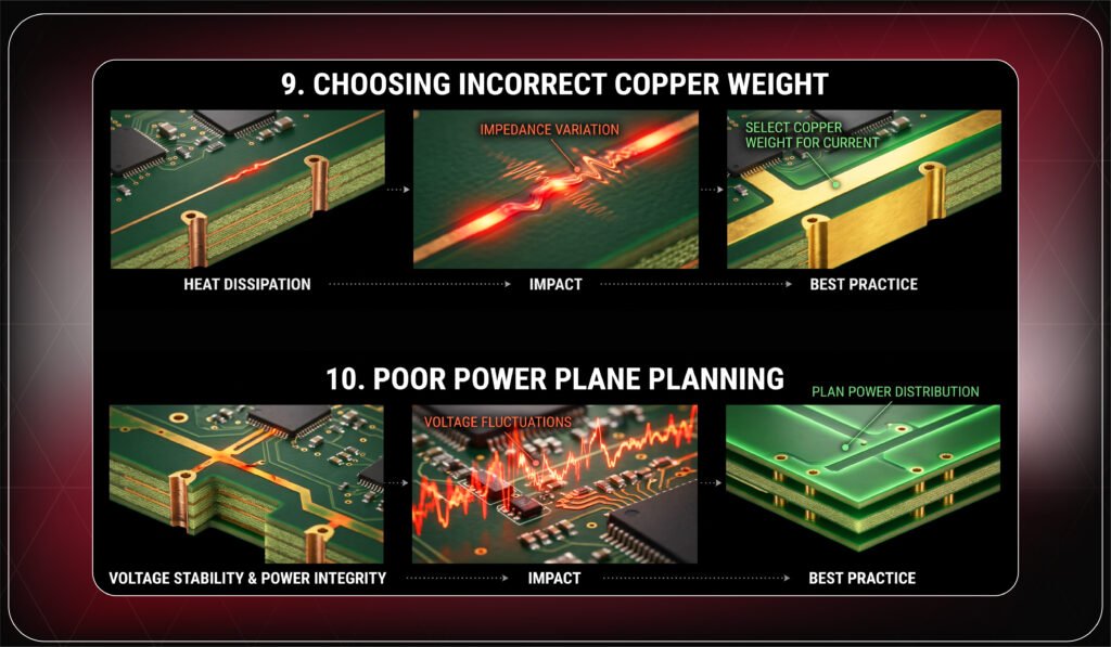
9. Choosing Incorrect Copper Weight
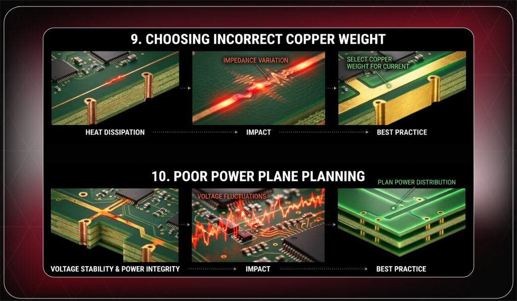
Copper thickness affects current capacity, heat dissipation, impedance, and manufacturability.
Impact:
- Impedance variation
- Thermal problems
- Higher fabrication complexity
Best practice:
Select copper weight according to current requirements and manufacturer capability.
10. Poor Power Plane Planning
Power planes influence voltage stability and power integrity, especially in high-speed designs.
Impact:
- Voltage fluctuations
- Power noise
- Reliability issues
Best practice:
Plan power distribution with proper plane design and effective decoupling.
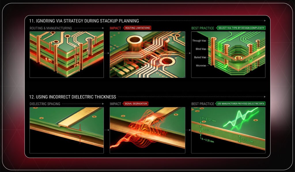
11. Ignoring Via Strategy During Stackup Planning
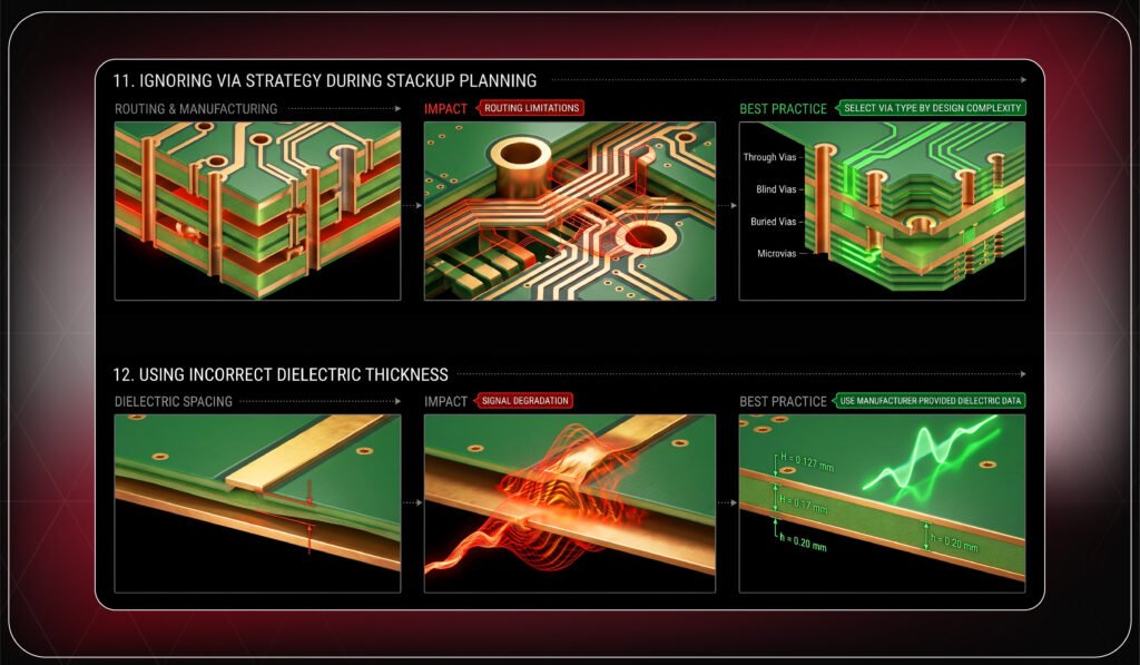
Via structures should be considered early because they affect routing and manufacturing.
Impact:
- Routing limitations
- Increased cost
- Fabrication challenges
Best practice:
Choose through vias, blind vias, buried vias, or microvias based on design complexity.
12. Using Incorrect Dielectric Thickness
Dielectric spacing directly affects impedance calculations and signal performance.
Impact:
- Impedance mismatch
- Signal degradation
- Timing issues
Best practice:
Use manufacturer-provided dielectric information for accurate simulation and fabrication.
13. Overlooking Copper Balance
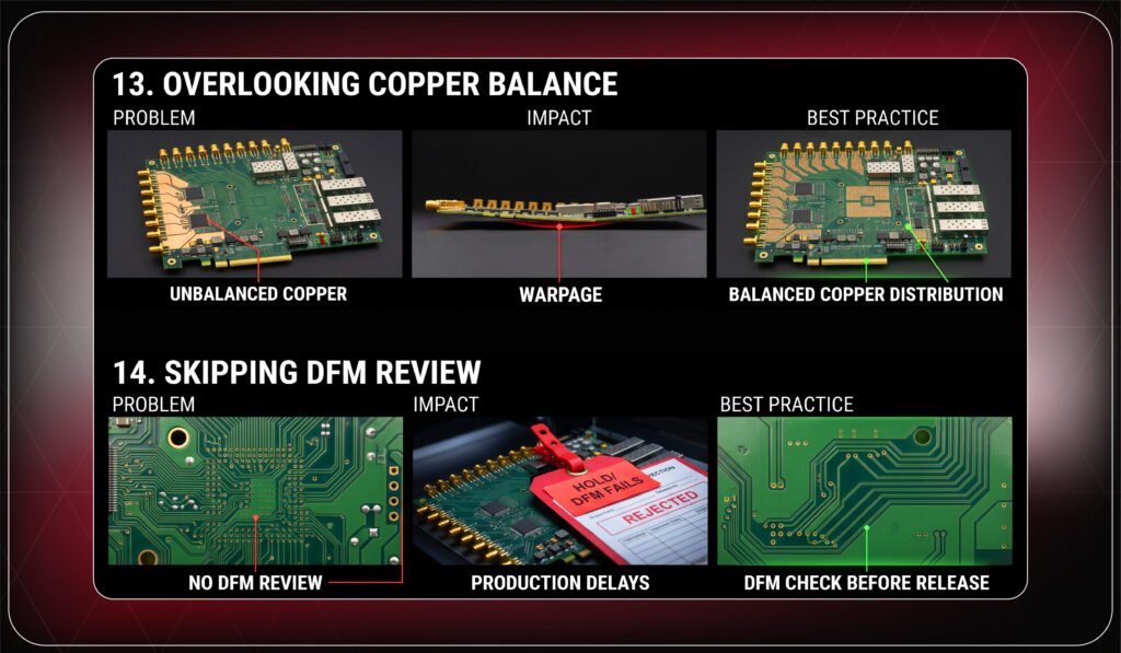
Large differences in copper density between layers can create stress during manufacturing.
Impact:
- Warpage
- Registration issues
- Reduced yield
Best practice:
Maintain balanced copper distribution across all layers.
14. Skipping DFM Review
A stackup may work electrically but fail during manufacturing if fabrication limits are ignored.
Impact:
- Production delays
- Design changes
- Lower first-pass success
Best practice:
Perform DFM checks before final release.
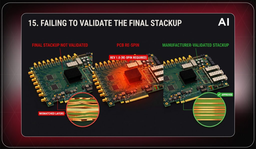
15. Failing to Validate the Final Stackup
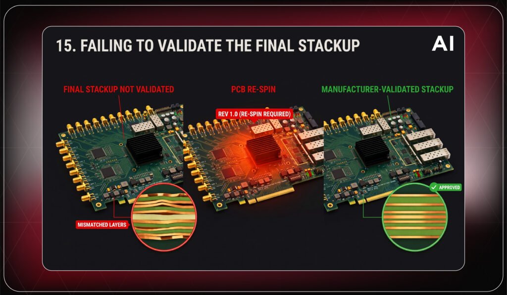
Releasing a design without final validation can introduce unexpected manufacturing problems.
Impact:
- PCB re-spins
- Increased cost
- Longer development cycles
Best practice:
Review the final stackup with the manufacturer before production.
PCB Stackup Design Checklist
Before releasing your design, verify:
- Layer count is finalized
- Manufacturer approval is completed
- Controlled impedance requirements are defined
- Ground and power planes are optimized
- Material selection matches operating conditions
- Copper balance is maintained
- Dielectric thickness is validated
- Via strategy is finalized
- DFM review is completed
Final Thought
A reliable PCB starts with a well-planned PCB Layer Stackup. The decisions made before routing influence signal integrity, power performance, EMI behavior, thermal stability, and manufacturing success.
By avoiding these 15 common stackup mistakes, hardware teams can reduce PCB re-spins, improve DFM, and increase the chances of achieving first-pass manufacturing success.
A carefully reviewed stackup is one of the most important steps toward building reliable electronic products.
Avoid costly PCB re-spins.
Get your stackup reviewed today.
Want to avoid hidden issues in your design?
Connect with us for the expert free consultation
https://calendly.com/gighz/30min
Frequently Asked Questions
1. What is a PCB stackup?
A PCB stackup is the arrangement of copper layers, dielectric materials, and insulating layers inside a multilayer circuit board.
2. Why should stackup planning happen before routing?
Because layer structure affects routing, impedance control, signal quality, and manufacturing feasibility.
3. How does stackup design improve reliability?
A properly planned stackup helps control electrical performance, reduce manufacturing problems, and improve product reliability.
Stuck in a loop of challenges? Always pick smart solution that works
Have you faced costly rework because 2D drawings skipped in MCAD workflows?
Effective way to prevent MCAD documentation errors recalls?
Please answer both poll questions before submitting.
Thank you for your response! 😊
Latest Post
Get Customized Engineering CAD Design Service

Book a Free Consultation Call
Partner with Gighz and bring your most innovative design concepts to life. Our engineering cad services accelerate development so you can focus on your big vision.
