


Your Mixed-Signal PCB Passed Every Test—So Why Are the Readings Still Unstable?
Your PCB powers up, the layout passes DRC, and manufacturing is complete.
Yet during testing, ADC readings fluctuate, sensors become inaccurate, or audio signals contain unwanted noise.
What caused the problem?
In many cases, the issue isn’t the schematic—it’s the PCB layout. Poor grounding, routing, or component placement allows digital switching noise to interfere with sensitive analog circuits.
Reducing noise in mixed-signal PCB designs requires careful planning of grounding, routing, power distribution, and component placement.
Getting this right early improves signal integrity, measurement accuracy, and overall PCB reliability.
What Is a Mixed-Signal PCB?

A mixed-signal PCB combines analog and digital circuits on the same board. Analog circuits process continuous signals such as sensor outputs, while digital circuits handle high-speed data from processors, memory, and communication interfaces.
Common applications include:
- Medical devices
- Industrial automation
- Automotive electronics
- IoT products
- Audio equipment
- Data acquisition systems
Although integrating both circuits reduces board size and cost, it also creates a challenge. Fast-switching digital signals generate electrical noise that can interfere with nearby analog circuits.
For example, an ADC connected to a pressure sensor may produce unstable readings because a high-speed clock trace is routed too close to its analog input. The schematic is correct, but the PCB layout allows unwanted interference.
Understanding where this noise originates is the first step toward reducing it.
Why Noise Becomes a Problem

Every digital IC switch thousands to millions of times per second, creating transient currents that travel through the PCB’s power and ground network. If these currents share return paths with sensitive analog signals, electrical noise is introduced into the circuit.
Common effects include:
- Unstable ADC readings
- Sensor inaccuracies
- Audio distortion
- Communication errors
- Increased EMI
- Reduced PCB reliability
As PCB complexity and signal speeds increase, controlling noise becomes even more important. Fortunately, most problems can be avoided by following proven PCB layout practices.
Key Techniques to Reduce Noise
1. Separate Analog and Digital Sections

The first step is to physically separate noisy digital circuits from sensitive analog circuitry. This reduces the chance of digital switching noise coupling into low-level analog signals.
For better isolation:
- Group analog components together.
- Keep processors and memory away from analog inputs.
- Place switching regulators away from precision circuits.
- Locate ADCs and DACs close to sensors.
Good partitioning simplifies routing and creates cleaner return-current paths.
2. Use Proper Grounding
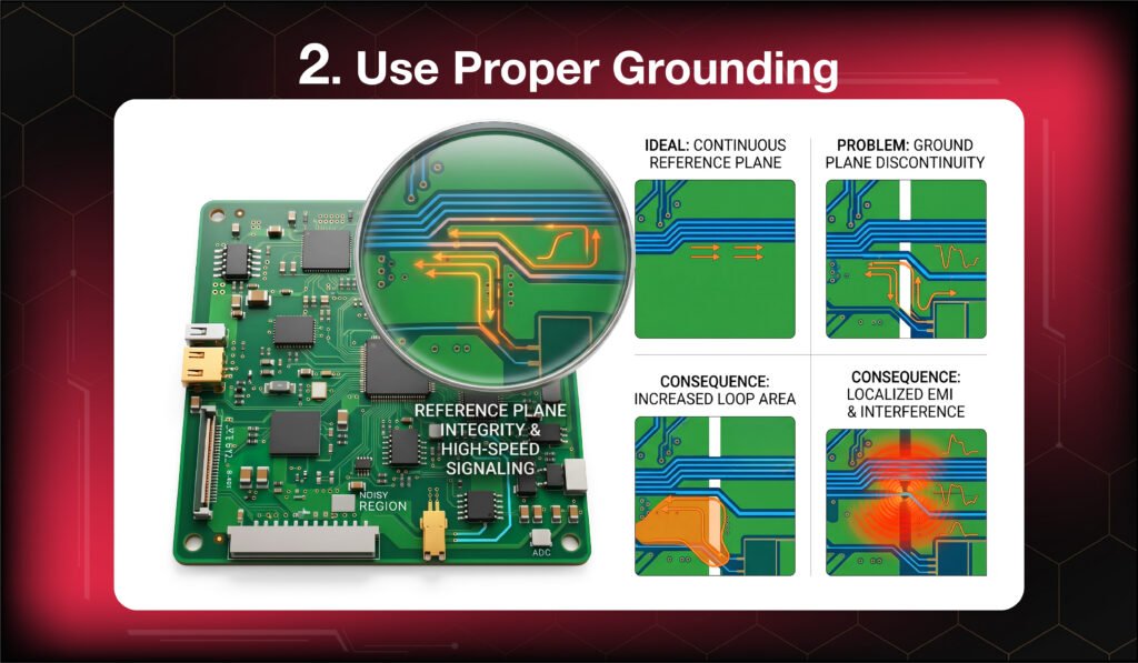
Grounding is one of the most important aspects of mixed-signal design.
A continuous ground plane provides a low-impedance return path for signals and minimizes ground noise. If high-speed traces cross plane gaps, return currents are forced to take longer paths, increasing loop area, EMI, and signal interference.
A well-planned grounding strategy improves both signal integrity and measurement accuracy.
3. Optimize Component Placement
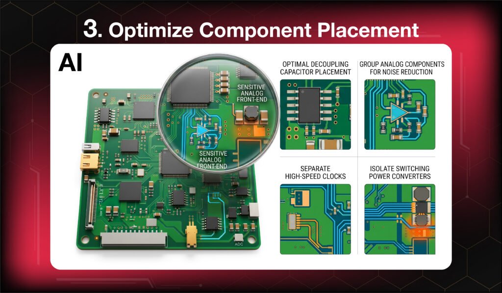
Good placement reduces noise before routing even begins.
Follow these guidelines:
- Place decoupling capacitors close to IC power pins.
- Keep analog components together.
- Separate clock generators from analog circuitry.
- Position power converters away from sensitive signals.
For example, placing a switching regulator beside an analog amplifier can introduce ripple into the signal path, reducing measurement accuracy.
Once placement is optimized, focus on delivering clean power.
4. Improve Power Integrity

Power supply noise directly affects analog performance.
Each time a digital IC switches, it draws a short burst of current. Without proper decoupling, these current spikes create voltage ripple that can affect nearby analog circuits.
To improve power integrity:
- Use adequate decoupling capacitors.
- Keep power traces short and wide.
- Minimize power distribution impedance.
- Isolate sensitive analog supplies where necessary.
Stable power delivery improves signal quality and reduces electrical noise.
5. Route Signals Carefully
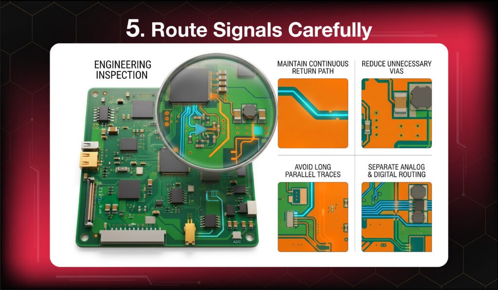
Routing decisions have a significant impact on PCB performance.
Keep analog traces short and avoid routing them parallel to high-speed clocks or switching power traces.
Best practices include:
- Maintain continuous return paths.
- Reduce unnecessary vias.
- Avoid long parallel traces.
- Separate analog and digital routing.
These techniques reduce crosstalk and improve signal integrity.
6. Control High-Speed Signals
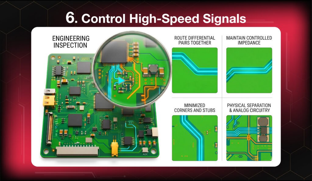
Interfaces such as DDR, USB, PCIe, Ethernet, and SERDES generate fast edge transitions that can become major noise sources.
To reduce interference:
- Route differential pairs together.
- Maintain controlled impedance.
- Minimize sharp corners and stubs.
- Keep high-speed traces away from analog circuits.
Proper routing reduces reflections, EMI, and signal distortion.
7. Verify the Layout Before Fabrication
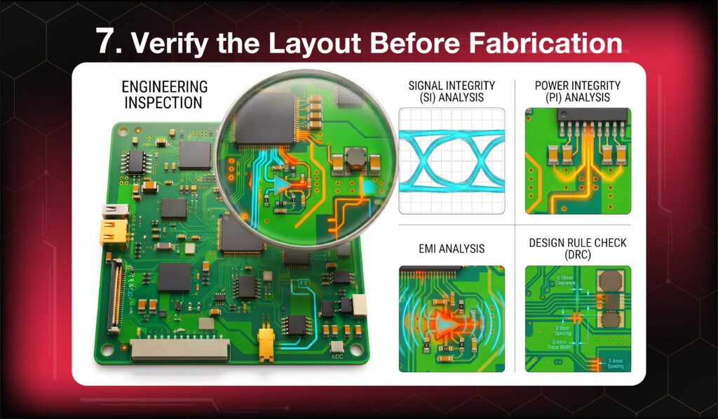
Even experienced designers validate their layouts before manufacturing.
Review the PCB using:
- Signal Integrity (SI) analysis
- Power Integrity (PI) analysis
- EMI analysis
- Design Rule Check (DRC)
These checks help detect grounding, routing, power, and high-speed signal issues before fabrication.
Common Design Mistakes
During the review, pay close attention to:
- Poor grounding
- Clocks routed near analog traces
- Incorrect decoupling placement
- Broken return paths
- Poor power distribution
- Skipping SI and PI analysis
Fixing these issues early helps prevent noise, EMI, and costly PCB re-spins.
Applying the following best practices helps prevent these problems during the design stage.
Best Practices
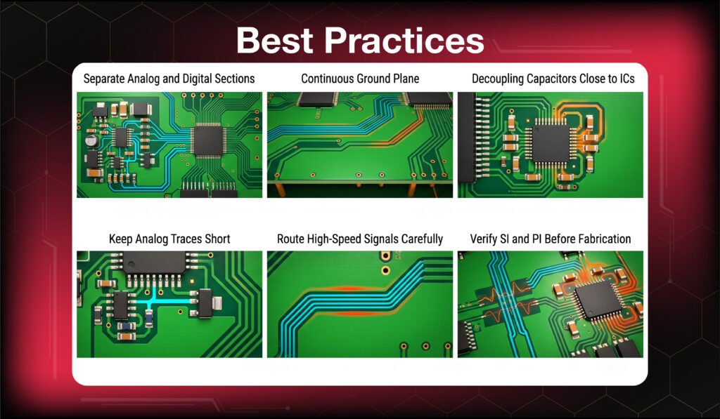
- Separate analog and digital sections.
- Use a continuous ground plane.
- Place decoupling capacitors close to ICs.
- Keep analog traces short.
- Route high-speed signals carefully.
- Verify SI and PI before fabrication.
- Review manufacturability before Gerber release.
Following these practices improves signal integrity, manufacturing success, and long-term PCB reliability.
Final Thought
Reducing noise in mixed-signal PCB designs requires more than separating analog and digital circuits. Reliable performance depends on proper grounding, optimized placement, clean routing, stable power delivery, and thorough design verification.
By addressing these factors early in the PCB layout process, engineers can reduce electrical noise, improve measurement accuracy, minimize EMI, and avoid costly PCB re-spins.
Want to avoid hidden issues in your design?
Connect with us for the expert free consultation
https://calendly.com/gighz/30min
Stuck in a loop of challenges? Always pick smart solution that works
Have you faced costly rework because 2D drawings skipped in MCAD workflows?
Effective way to prevent MCAD documentation errors recalls?
Please answer both poll questions before submitting.
Thank you for your response! 😊
Latest Post
Get Customized Engineering CAD Design Service

Book a Free Consultation Call
Partner with Gighz and bring your most innovative design concepts to life. Our engineering cad services accelerate development so you can focus on your big vision.
