

Why Are Reference Plane Critical for High-Speed PCB Design?
- Posted On:
- September 25, 2026
- Category:
- Ecad
The Signal Is Only Half the Story.
A high-speed signal may travel along a perfectly routed trace, but that is only half of its journey.
The other half flows beneath the trace through a continuous reference plane that carries return current.
At low frequencies, this path may seem easy to overlook. As edge rates increase, even a small interruption can alter the interconnect’s behavior. Gaps, splits, layer transitions, or poor stack-up planning can force current to detour, increasing loop inductance and electromagnetic coupling.
The result may include reflections, crosstalk, EMI, timing errors, and signal integrity failures.
The trace and its return path form one electrical system, making this relationship essential for reliable DDR5, PCIe, USB4, Ethernet, and HDMI designs.
What Is a Reference Plane in High-Speed PCB Design?
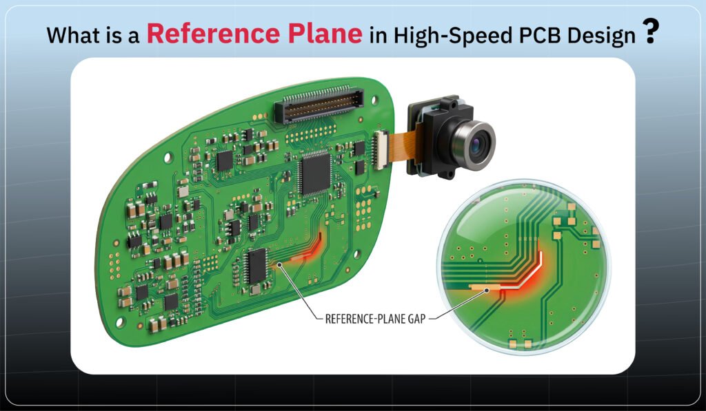
A reference plane is a continuous copper layer, usually a ground or power plane, placed next to a signal layer. Its primary role is to provide the return current path for high-speed signals.
At high frequencies, return current flows directly beneath the signal trace along the path of lowest impedance, creating a compact current loop.
This minimizes inductance, maintains controlled impedance, and improves overall signal quality.
How Does Plane Continuity Improve Signal Integrity?
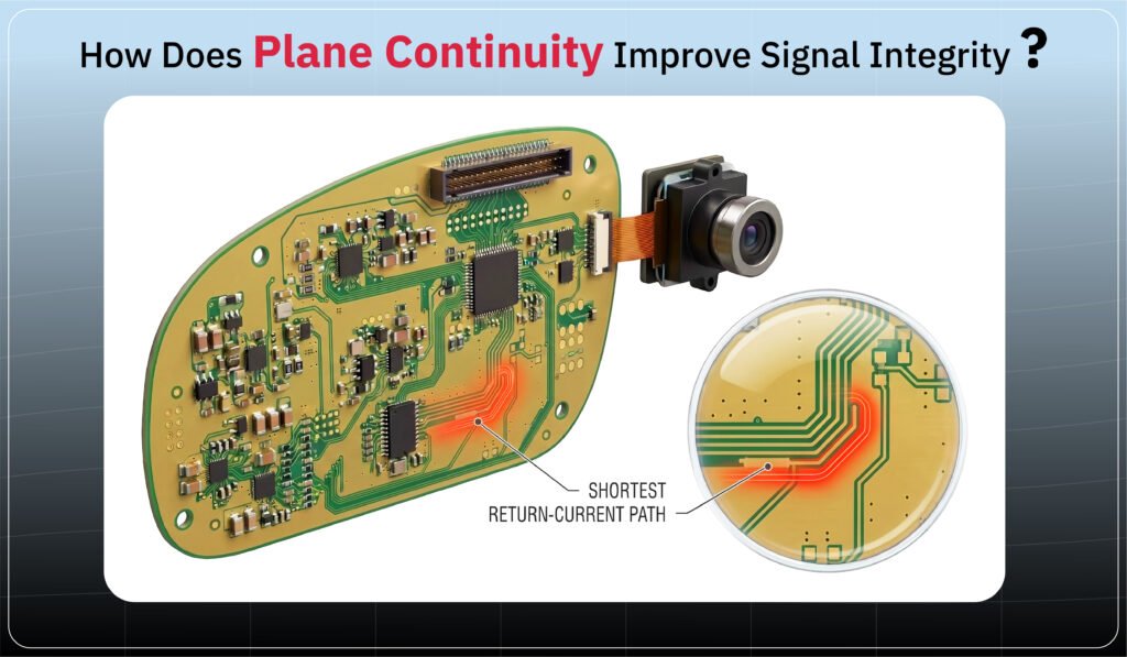
High-speed signals depend on a stable electrical environment.
A continuous ground plane keeps electromagnetic fields tightly coupled to the signal trace, ensuring predictable impedance throughout the routing path.
When the ground plane remains continuous:
- Return current follows the shortest path.
- Controlled impedance stays consistent.
- Signal reflections are minimized.
- Crosstalk between adjacent traces is reduced.
- EMI emissions decrease.
- High-speed signals are less likely to encounter return-path discontinuities.
However, when this copper layer is interrupted, return current is forced to take a longer path. The larger current loop increases inductance, creates impedance discontinuities, and degrades signal quality.
This is why interfaces such as DDR5, PCIe, USB4, Ethernet, HDMI, and RF circuits rely on continuous ground planes and proper stack-up planning.
What Happens If a High-Speed Trace Crosses a Split Plane?
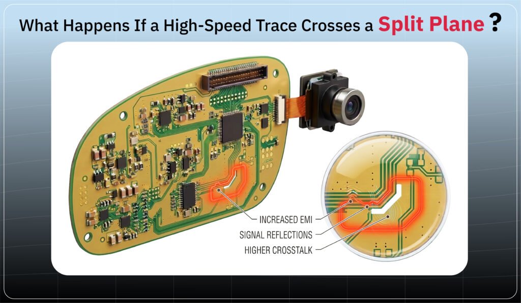
Routing a high-speed signal across a split or gap in the ground plane is one of the most common PCB layout mistakes.
Although the trace itself remains continuous, the return current can no longer flow directly beneath it. Instead, it detours around the gap, creating a much larger current loop.
The consequences include:
- Increased electromagnetic interference (EMI)
- Signal reflections
- Higher crosstalk
- Timing errors
- Reduced signal integrity
- Compliance test failures
For example, a USB 3.x differential pair routed across a split ground plane may work during functional testing but fail EMI certification because the interrupted return path increases electromagnetic radiation. Similar issues are common in DDR memory, PCIe, and high-speed Ethernet designs.
How Does PCB Stack-Up Affect Signal Performance?
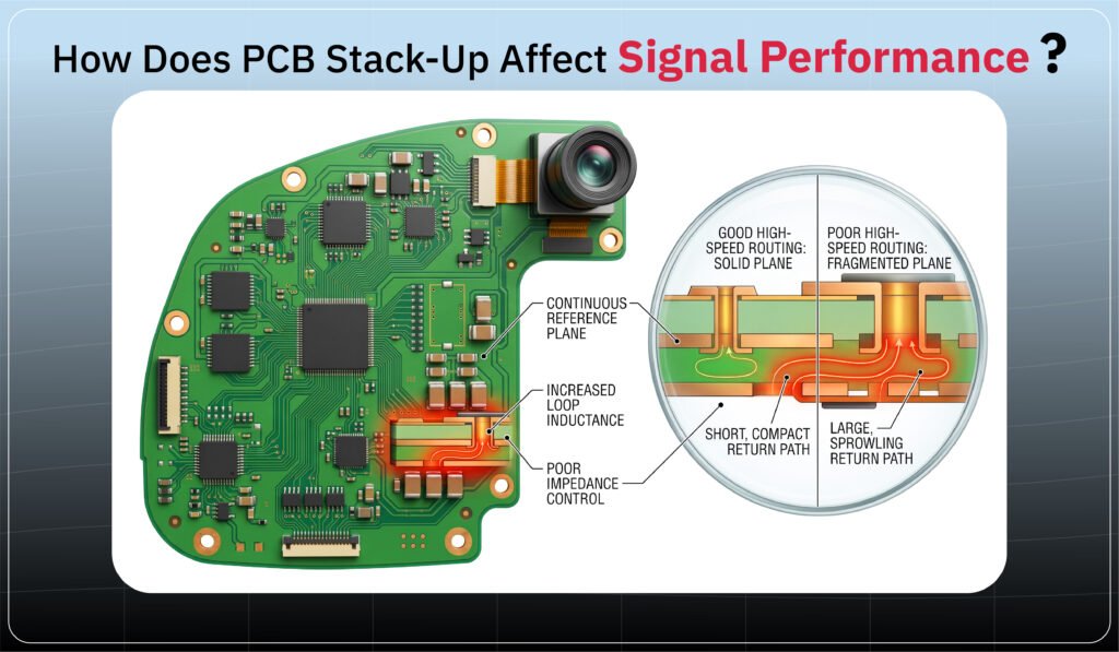
Signal performance is determined long before routing begins.
A properly planned PCB stack-up places every critical signal layer next to a continuous ground plane. This arrangement keeps return current close to the signal path, improves impedance control, and minimizes electromagnetic noise.
Poor stack-up planning often forces signals to reference distant or fragmented copper layers, increasing loop inductance and making impedance much harder to control.
Whether designing a simple four-layer board or a complex multilayer PCB, stack-up planning should always prioritize continuous copper layers beneath high-speed signals.
Can a Power Plane Replace a Ground Plane?
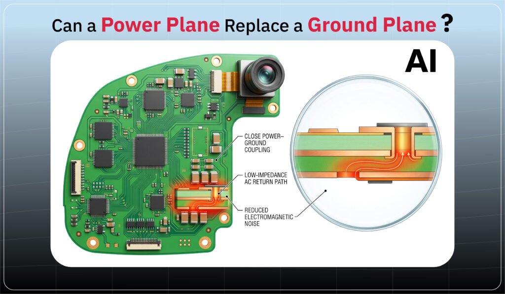
Yes—but only under the right conditions.
A power plane can serve as an effective AC return path when it is closely coupled to a solid ground plane through a thin dielectric layer and supported by properly placed decoupling capacitors.
Without this close coupling, it cannot provide the low-impedance path required for high-speed signals. For most designs, a continuous ground plane remains the preferred solution.
Why Are Stitching Vias Important?
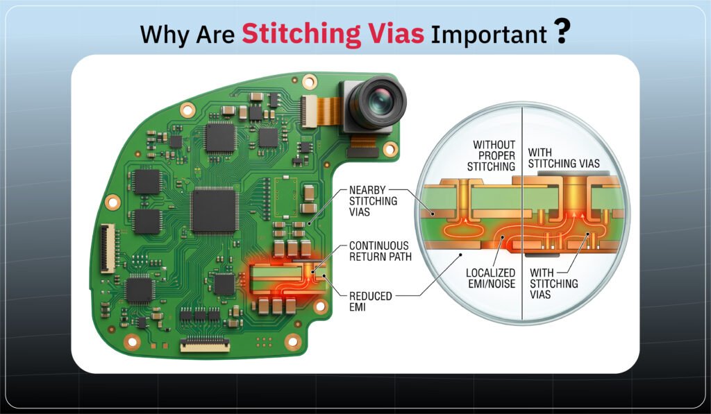
High-speed signals frequently change layers through vias.
When this occurs, the return current must also transition to the adjacent ground layer. Without nearby stitching vias connecting the ground layers, the return path becomes longer, increasing inductance, noise, and EMI.
Placing stitching vias close to signal transitions helps maintain a continuous current path and preserves signal integrity throughout the PCB.
Best Practices for Return Current Management
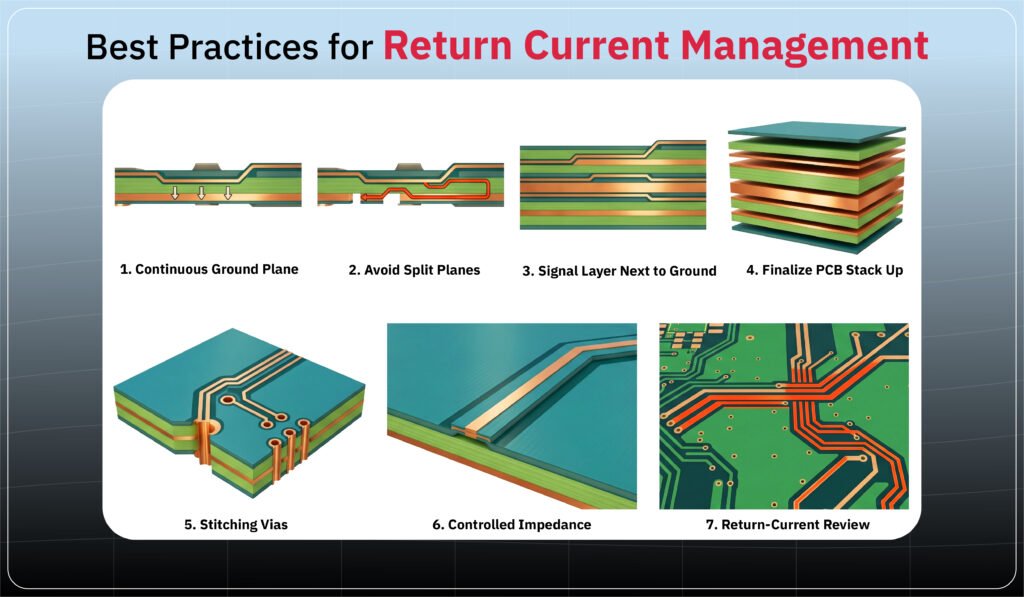
Follow these best practices to improve high-speed PCB performance:
- Use continuous ground planes beneath critical signals.
- Avoid routing traces across split or fragmented copper areas.
- Place every high-speed signal layer next to a solid ground layer.
- Finalize the PCB stack-up before routing begins.
- Add stitching vias near layer transitions.
- Verify controlled impedance using the final stack-up.
- Review returns current paths during every PCB design review.
Following these practices improves signal integrity, reduces EMI, and increases the likelihood of first-pass hardware success.
Final Thought
Reference plane are not passive copper layers hidden inside a PCB—they are a fundamental part of every high-speed signal path.
They guide return current, stabilize controlled impedance, reduce EMI, and preserve signal integrity across interfaces such as DDR5, PCIe, USB4, Ethernet, HDMI, and RF circuits.
No matter how carefully a PCB is routed, its performance ultimately depends on the quality and continuity of the ground plane beneath the signal traces.
Treating this layer as a critical design element—not an afterthought—can reduce costly re-spins, improve first-pass success, and deliver reliable high-speed PCB performance.
Prevent EMI issues with expert high-speed PCB validation.
Start Your PCB Design Review →https://gighz.net/contact-us/
Book a Call. Schedule a Free Consultation now. https://calendly.com/gighz/30min
Stuck in a loop of challenges? Always pick smart solution that works
Have you faced costly rework because 2D drawings skipped in MCAD workflows?
Effective way to prevent MCAD documentation errors recalls?
Please answer both poll questions before submitting.
Thank you for your response! 😊
Latest Post
Get Customized Engineering CAD Design Service

Book a Free Consultation Call
Partner with Gighz and bring your most innovative design concepts to life. Our engineering cad services accelerate development so you can focus on your big vision.
