

High-density PCB design has become a core requirement in modern electronics.
As devices become smaller and more powerful, engineers are expected to fit more functionality into less space without compromising performance, reliability, or manufacturability.
This shift sounds simple on paper.
In reality, it introduces a set of serious design challenges that affect routing, signal behavior, heat management, and production outcomes.
This blog explains those challenges in a practical way and shows how to manage them using real PCB design thinking.
Understanding High-Density PCB Design and Its Growing Importance
High-Density Interconnect (HDI) PCB design refers to boards with higher wiring density per unit area using advanced fabrication technologies such as microvias, blind and buried vias, fine trace geometry, and sequential lamination.
The goal is not only miniaturization but also maintaining high performance, signal integrity, and reliability in a smaller footprint. However, as density increases, design complexity also rises significantly.
The demand for HDI is growing due to shrinking consumer electronics, higher performance expectations, and the rise of high-speed communication systems.
Technologies like IoT, AI hardware, and electric vehicles require compact yet powerful designs.
This forces engineers to create smaller PCBs with greater functionality, making HDI design essential in modern electronics.
Challenge 1: Routing Congestion in Tight Layouts
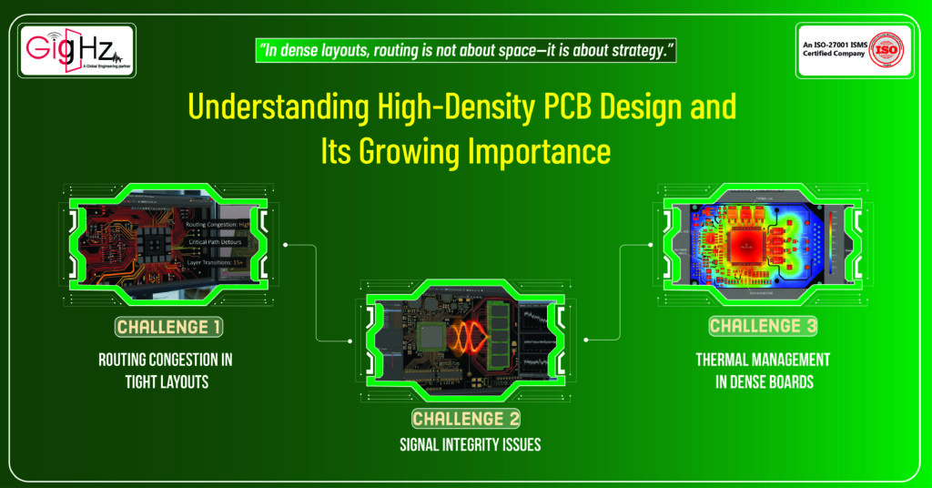
One of the first issues in HDI design is routing congestion. When too many components are placed in a small area, there is limited space for traces to pass through.
This leads to:
- Complex routing paths
- Longer trace detours
- Difficulty in maintaining clean signal flow
- Increased risk of layout errors
When routing becomes crowded, even simple design changes can affect multiple signal paths.
How to manage it:
The key is to focus on placement before routing:
- Group components based on function
- Keep related circuits physically close
- Align components with natural signal flow direction
- Avoid random placement across the board
Good placement reduces routing complexity significantly. In many cases, it prevents congestion before it even starts.
Challenge 2: Signal Integrity Issues
As trace density increases, signals start interacting with each other.
This leads to signal integrity problems such as:
- Crosstalk between adjacent traces
- Impedance mismatch
- Signal reflection at vias and connectors
- Timing delays in high-speed paths
These issues become more serious as operating frequencies increase.
Challenge 3: Thermal Management in Dense Boards
When components are tightly packed, heat does not spread easily. This creates localized hot spots that can affect performance and reliability.
Common thermal issues include:
- Overheating of power components
- Uneven temperature distribution
- Reduced lifespan of sensitive components
- System instability under load
The challenge becomes worse when multiple high-power components are placed close together.
How to manage it:
Thermal control should be part of the layout strategy:
- Spread heat-generating components instead of clustering them
- Use thermal vias to transfer heat across layers
- Increase copper areas for heat dissipation
- Keep high-power components away from sensitive areas
- Ensure proper heat flow paths across the board
Good thermal design improves both performance and long-term reliability.
Challenge 4: Power Distribution Problems
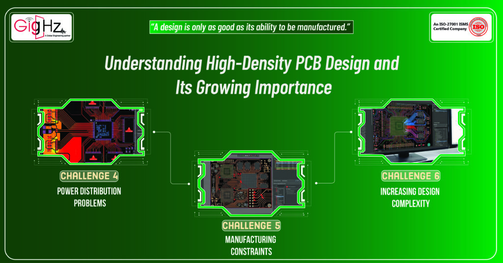
In high-density designs, power delivery becomes more complex.
Long or narrow power paths can cause:
- Voltage drops
- Power noise
- Ground instability
- Interference between sections of the circuit
These issues can lead to unpredictable system behavior.
How to manage it:
A stable power network requires careful planning:
- Use solid ground planes instead of fragmented routing
- Keep power paths short and wide
- Place decoupling capacitors close to IC power pins
- Separate noisy power sections from sensitive analog sections
- Ensure proper return path design for all signals
A well-designed power system is critical for stable PCB performance.
Challenge 5: Manufacturing Constraints
High-density PCB design often pushes manufacturing limits. Very fine traces, tight spacing, and microvias require precise fabrication processes.
Common manufacturing issues include:
- Fabrication limitations on trace width and spacing
- Via reliability concerns
- Assembly difficulties in dense layouts
- Higher rejection rates during production
How to manage it
Design must align with manufacturing capability:
- Follow Design for Manufacturing (DFM) guidelines
- Avoid pushing minimum fabrication limits unnecessarily
- Validate spacing and clearance using design rule checks
- Keep stack-up design realistic and manufacturable
- Coordinate early with fabrication requirements
A good design is not only functional but also manufacturable at scale.
Challenge 6: Increasing Design Complexity
High-density PCB projects often become difficult to manage due to:
- Large number of interconnections
- Multiple layers with complex routing
- Tight spacing constraints
- Frequent design iterations
Without structure, the design process becomes error-prone.
How to manage it
A structured approach is essential:
- Divide the board into functional blocks
- Work step-by-step: placement, routing, optimization
- Avoid making large changes late in the design stage
- Keep design documentation organized
- Use consistent naming and labeling practices
Clear structure reduces confusion and improves design accuracy
Final Thought
High-density PCB design is not just about fitting more components into a smaller area.
It is about maintaining a balance between performance, reliability, thermal control, signal integrity, and manufacturability.
The main challenges—routing congestion, signal integrity, thermal buildup, power distribution issues, and manufacturing limits—are all connected to one central idea: managing complexity in limited space.
With a structured design approach and careful planning at each stage, these challenges can be controlled effectively. In modern electronics, this ability is becoming less of an advantage and more of a necessity.
It represents the future of electronics, and mastering it requires both technical knowledge and disciplined design thinking.
Need help with high-density PCB design challenges?
Contact us for guidance and practical PCB design solutions.
Book a Call. Schedule a Free Consultation now. https://calendly.com/gighz/30min
Stuck in a loop of challenges? Always pick smart solution that works
Have you faced costly rework because 2D drawings skipped in MCAD workflows?
Effective way to prevent MCAD documentation errors recalls?
Please answer both poll questions before submitting.
Thank you for your response! 😊
Latest Post
Get Customized Engineering CAD Design Service

Book a Free Consultation Call
Partner with Gighz and bring your most innovative design concepts to life. Our engineering cad services accelerate development so you can focus on your big vision.
