

Zuken vs Altium: A Practical Comparison for EDA Conversion
- Posted On:
- August 20, 2026
- Category:
- Ecad
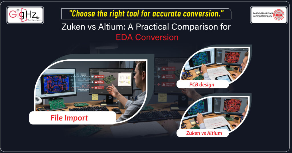
When working on PCB designs, switching between tools is sometimes unavoidable.
Maybe your client uses a different platform, or your team is upgrading tools.
That’s where EDA conversion comes in.
But here’s the truth—EDA conversion is not just “file import.”
It’s about preserving the intelligence of your design.
Every PCB design carries critical data like connectivity, constraints, stack-up, and component mapping.
If any of this break during conversion, you’re not just fixing files—you’re redesigning.
This is why choosing between tools like Zuken vs Altium Designer becomes very important.
Let’s break it down in a simple, practical way.
Zuken vs Altium: What’s the Real Difference in EDA Conversion?
When you convert a design, the tool has to translate multiple layers of data:
- Schematic data → symbols, nets, hierarchy
- PCB layout → routing, vias, copper shapes
- Design rules → spacing, width, constraints
- Component data → footprints, libraries, parameters
If even one layer doesn’t translate correctly, issues start appearing like:
- Missing nets
- Incorrect footprints
- Broken hierarchy
- DRC (Design Rule Check) errors
So, the real goal is not just conversion—it’s data integrity after conversion.
How Altium Handles EDA Conversion
Altium Designer is built with a unified design architecture, which plays a big role in conversion quality.
Here’s how it technically improves the process:
1. Multi-format Import Engine
Altium supports importing from multiple ECAD tools.
During this process, it maps:
- Nets → preserved with connectivity logic
- Components → linked with library references
- Layout → translated into Altium’s native PCB engine
This reduces the chance of losing connections or structure.
2. Intelligent Component Mapping
During conversion, mismatched components are common.
Altium handles this using:
- Built-in component libraries
- Parameter-based matching (name, value, footprint)
This allows faster alignment of correct models without heavy manual replacement.
3. Layer Stack & Impedance Control
Modern PCBs rely heavily on layer stack definitions and impedance control.
Altium includes:
- Layer Stack Manager
- Built-in field solver
So, after conversion, you can verify stack-up and impedance values immediately, instead of recalculating from scratch.
4. Integrated Design Rule System
Altium automatically applies and checks:
- Clearance rules
- Routing constraints
- Width and via rules
This ensures that after conversion, your design is still manufacturing-ready.
5. Signal Integrity Awareness

For high-speed designs, conversion must preserve signal paths.
Altium supports:
- Basic signal integrity checks
- Controlled routing validation
This helps maintain integrity of critical nets like differential pairs.
6. Unified Environment
Everything—schematic, PCB, libraries, and outputs—is handled in one platform.
That means:
- No switching tools
- No data mismatch between modules
- Faster validation after conversion
In short, Altium focuses on preserving design intelligence while reducing manual effort during conversion.
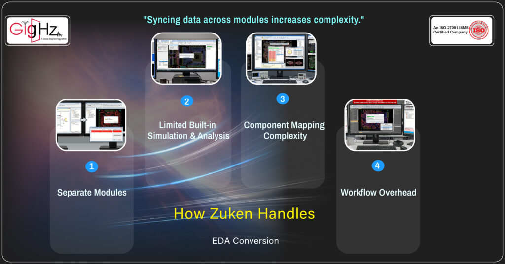
How Zuken Handles EDA Conversion
Zuken is built for structured, high-complexity PCB workflows, commonly used in enterprise and system-level design environments.
Its modular architecture handles schematic, layout, and verification separately, which gives strong process control but adds coordination during conversion.
1. Separate Modules
Schematic, layout, and other features may work as separate modules.
During conversion, this can lead to:
- Extra steps to sync data
- More manual validation
This increases coordination effort during conversion.
2. Limited Built-in Simulation & Analysis
Compared to Altium, Zuken has fewer built-in tools for:
- Signal integrity
- Advanced simulation
- Field solving
So, engineers may need external tools to verify designs after conversion.
3. Component Mapping Complexity
Component libraries are not as tightly integrated.
This can result in:
- More manual footprint matching
- Increased risk of mismatched components
This adds additional effort during component alignment.
4. Workflow Overhead
Because of its structure, users may need to:
- Export/import between modules
- Perform separate checks
This increases overall conversion time.
In short, Zuken can handle conversion, but it often requires more manual work to ensure accuracy.
How to Choose the Right PCB Design Approach
From a practical perspective, choosing between Zuken vs Altium depends on project requirements and workflow structure rather than a fixed preference.
Different projects prioritize different factors:
- Some focus on strict process control and structured workflows
- Others focus on integrated environments and faster iteration
- Some require heavy validation stages, while others prioritize speed
The choice is generally influenced by:
- Project size and complexity
- Workflow structure
- Team collaboration model
- Conversion accuracy needs
- Validation requirements
In real engineering scenarios, both approaches are valid—the key is alignment with the project environment.
Final Thoughts
In a Zuken vs Altium comparison, EDA conversion is not just a small step—it directly affects your time, cost, and product quality.
Even small mistakes can lead to rework, delays, and added effort.
That’s why choosing the right platform matters. It’s not just about opening files, but keeping your design accurate and ready for manufacturing.
While Zuken offers flexibility, it often requires more manual work after conversion. This can slow things down, especially in complex projects.
On the other hand, Altium Designer makes the process smoother. With its unified environment and built-in validation, you can move to production faster with fewer errors.
If your goal is to save time and reduce errors, choosing the right tool can significantly improve overall design efficiency.
Book a Call. Schedule a Free Consultation now. https://calendly.com/gighz/30min
Stuck in a loop of challenges? Always pick smart solution that works
Have you faced costly rework because 2D drawings skipped in MCAD workflows?
Effective way to prevent MCAD documentation errors recalls?
Please answer both poll questions before submitting.
Thank you for your response! 😊
Latest Post
Get Customized Engineering CAD Design Service

Book a Free Consultation Call
Partner with Gighz and bring your most innovative design concepts to life. Our engineering cad services accelerate development so you can focus on your big vision.
