12 PCB Design Tips for Reliable and High-Performance Electronics
- Posted On:
- May 4, 2026
- Category:
- Ecad

Reliable electronics begin with a well-planned PCB layout.
While schematics define how components are connected, it is the PCB layout that determines how those connections behave in real-world operation. Signal flow, power delivery, and return current paths are all shaped at the layout stage.
Even when a schematic is correct, poor layout decisions can lead to noise, signal distortion, EMI issues, and unstable system performance. These issues often appear only during testing or field operation, making them harder and more expensive to fix.
As electronic systems become faster, smaller, and more complex, PCB design discipline becomes even more important. Small layout mistakes can have a large impact on performance and reliability.
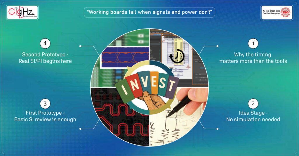
A simple principle to follow is:
Focus on placement first, then routing.
The following 12 practical PCB design tips will help improve reliability, reduce noise, and support high-performance electronics.
PCB Design Tips for Reliable Electronics
1. Optimise Your Layer Stack-Up
A well-designed PCB stack-up forms the foundation of signal integrity and power distribution.
It defines how signal layers interact with reference planes and ensures stable electrical behavior.
Do this:
- Place signal layers adjacent to ground planes
- Maintain consistent dielectric spacing
- Avoid unnecessary layer transitions
- Validate the stack-up with your manufacturer early
Why it matters:
A poorly planned stack-up can lead to impedance mismatches, signal reflections, and EMI issues that are difficult to correct later in the design cycle.
2. Control Impedance from the Start
Controlled impedance is essential in high-speed PCB design. Variations in impedance can distort signals and cause reflections.
Do this:
- Match trace width according to stack-up
- Maintain consistent spacing
- Use impedance calculators or simulation tools
- Keep differential pairs properly matched
Why it matters:
Even minor impedance variations can result in signal degradation, especially in high-speed communication systems.
3. Separate Analog and Digital Zones
Mixed-signal designs require careful separation to avoid interference between noisy digital circuits and sensitive analog components.
Do this:
- Physically separate analog and digital sections
- Avoid routing analog signals near switching circuits
- Use controlled grounding techniques
Why it matters:
Proper separation improves signal clarity and reduces noise-related performance issues.
4. Smart Component Placement
Component placement directly influences routing efficiency and signal behavior. Poor placement leads to longer traces and increased noise.
Do this:
- Place related components close together
- Keep high-speed components tightly grouped
- Follow natural signal flow direction
- Minimize unnecessary spacing
Why it matters:
Good placement simplifies routing and reduces the risk of signal integrity issues.
5. Use Short, Direct Routing
Trace routing plays a critical role in maintaining signal quality. Long or complex routing paths introduce delay and noise.
Do this:
- Keep high-speed traces as short as possible
- Avoid unnecessary bends and loops
- Minimize via usage
- Re-route placement if routing becomes complex
Why it matters:
Short and direct routing improves signal timing and reduces potential interference.
6. Maintain Clean Ground Planes
A continuous ground plane provides a stable return path for signals and helps control EMI.
Do this:
- Keep ground planes continuous
- Avoid splits under critical signal paths
- Maintain low-impedance return paths
Why it matters:
Interrupted ground paths can cause signal instability and increase electromagnetic interference.
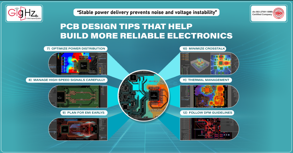
7. Optimize Power Distribution
Power integrity is essential for reliable circuit operation. Fluctuations in power can lead to unexpected behavior.
Do this:
- Place decoupling capacitors close to IC power pins
- Use dedicated power planes
- Reduce loop inductance
Why it matters:
Stable power delivery prevents voltage drops, noise, and system resets.
8. Manage High-Speed Signals Carefully
High-speed signals require careful handling to maintain timing accuracy and signal integrity.
Do this:
- Match trace lengths in critical paths
- Maintain symmetry in differential pairs
- Avoid routing near noisy circuits
- Keep signal paths clean and direct
Why it matters:
Improper handling of high-speed signals can lead to timing errors and data loss.
9. Plan for EMI Early
Electromagnetic interference should be considered early in the design process rather than addressed after issues arise.
Do this:
- Isolate noisy circuits from sensitive ones
- Maintain strong grounding strategy
- Add filtering components where needed
Why it matters:
Early EMI planning reduces redesign cycles and improves compliance with standards.
10. Minimize Crosstalk
Crosstalk occurs when signals interfere due to close proximity.
Do this:
- Maintain spacing between high-speed traces
- Avoid long parallel routing
- Use ground shielding if needed
Why it matters:
Reducing crosstalk improves signal clarity and overall system performance.
11. Thermal Management
Thermal performance affects both reliability and component lifespan.
Do this:
- Distribute heat-generating components evenly
- Use thermal vias and copper pours
- Design for airflow within the enclosure
Why it matters:
Proper heat management prevents overheating and improves long-term reliability.
12. Follow DFM Guidelines
Design for Manufacturing (DFM) ensures your PCB can be produced efficiently without errors.
Do this:
- Follow spacing and clearance rules
- Verify drill sizes and via structures
- Review pad and solder mask design
Why it matters:
DFM compliance reduces production issues and ensures smooth manufacturing.
Why PCB Layout Matters More Than Ever
PCB design is not just about connectivity — it is about controlling how the entire system behaves under real operating conditions.
A well-designed PCB ensures:
- Stable signal integrity
- Clean power delivery
- Reduced electromagnetic noise
- Better thermal performance
- Higher manufacturing success rate
Poor PCB layout, on the other hand, can cause repeated redesign cycles, performance issues, and increased development cost.
Final Thoughts
PCB design is more than connecting components—it is about ensuring stable, reliable performance under real-world conditions.
Successful designs are built on:
- Strong stack-up planning
- Controlled impedance
- Clean routing practices
- Stable power and grounding
These PCB design tips help reduce noise, improve signal quality, and build high-performance electronic systems that operate reliably.
Even small improvements in layout can lead to significant gains in performance and reliability. Planning early, validating designs, and following proven best practices will help you avoid costly redesigns and delays.
Book a Call. Schedule a Free Consultation now. https://calendly.com/gighz/30min
Stuck in a loop of challenges? Always pick smart solution that works
Have you faced costly rework because 2D drawings skipped in MCAD workflows?
Effective way to prevent MCAD documentation errors recalls?
Please answer both poll questions before submitting.
Thank you for your response! 😊
Latest Post
Get Customized Engineering CAD Design Service

Book a Free Consultation Call
Partner with Gighz and bring your most innovative design concepts to life. Our engineering cad services accelerate development so you can focus on your big vision.