Common Design Mistakes That Slow Down Student-Led Hardware Startup Companies
- Posted On:
- January 12, 2026
- Category:
- Ecad
Every student hardware team knows the excitement of building a new idea.
You sketch the system, design the PCB, send the files to fabrication — and wait for that first board with full hope.
But the moment testing begins, the excitement often shifts.
A signal is noisy, a regulator overheats, a connector doesn’t align, or the board behaves differently from what the simulation suggested.
These problems feel surprising, but they are actually very common in early-stage student projects.
They happen not because the design is weak, but because some important engineering steps were skipped or rushed — system-level planning, stack-up decisions, PDN thinking, simulations, library checks, and proper reviews.
This blog highlights the practical design mistakes that slow down student-led hardware startups companies and explains how to avoid them with simple, professional practices.
With the right process, your next prototype can move from “just working” to truly reliable.
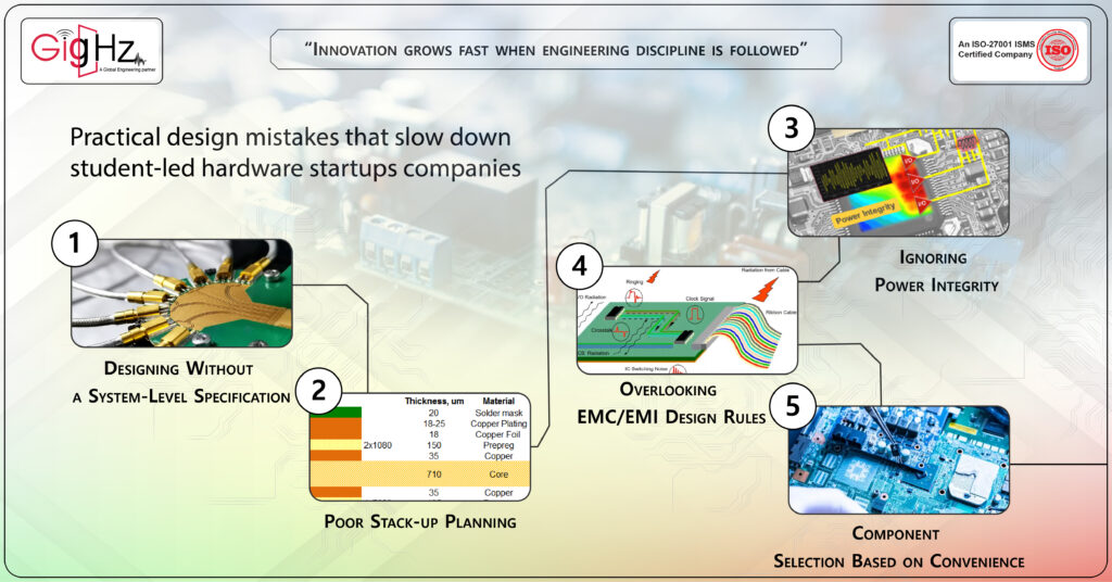
1. Designing Without a System-Level Specification
Many student startups start schematic design before defining functional requirements, power budgets, or interface dependencies.
This leads to:
- Unclear voltage domains between boards
- Conflicting I/O signal definitions
- Underestimated current draw or power dissipation
Professional Fix:
Before opening your EDA tool, create a System Design Specification (SDS) — detailing inputs/outputs, voltage rails, communication buses, operating temperature, and power envelopes.
This single document guides schematic capture, layout, and simulation.
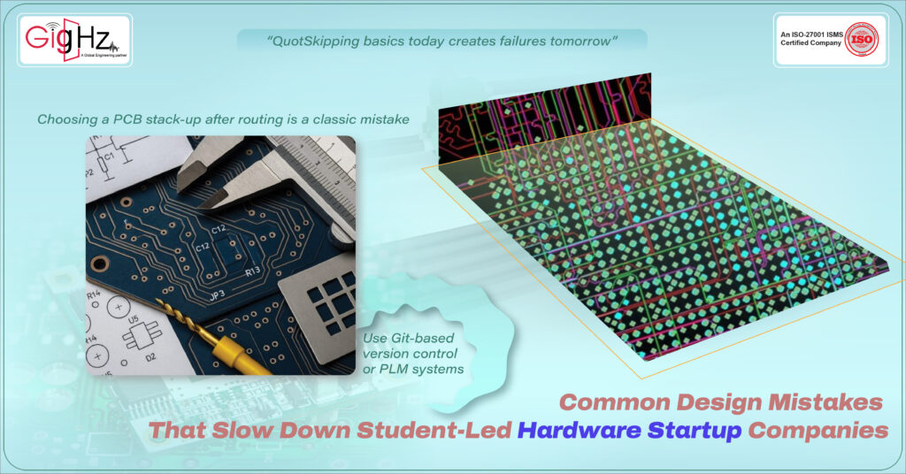
2. Poor Stack-up Planning
Choosing a PCB stack-up after routing is a classic mistake.
Without defined layer arrangement, dielectric thickness, and impedance targets, your traces won’t meet signal integrity or EMC goals.
Common student errors:
- Using a 2-layer board for high-speed designs
- No controlled impedance plan
- Missing return path continuity in ground layers
Professional Fix:
Always define the stack-up early with your fabricator. Use impedance calculators (like Polar Si9000 or Saturn PCB) to confirm trace widths for differential and single-ended signals.
3. Ignoring Power Integrity Early
Students often focus on signal routing but neglect power distribution network (PDN) design.
A poor PDN leads to noise coupling, jitter, or even IC malfunction under dynamic load.
Typical Mistakes:
- Random decoupling capacitor placement
- Long power traces with large voltage drops
- Missing ground stitching vias near return paths
Professional Fix:
Use Power Integrity (PI) simulation to validate voltage stability across loads.
Place decoupling capacitors by frequency range (bulk, mid, high) near IC power pins. Maintain low-impedance return loops.
4. Overlooking EMC/EMI Design Rules
EMC failures are a top reason prototypes fail compliance or behave erratically.
Students rarely apply return current path control, filtering, or shielding principles.
Common Oversights:
- Split ground planes under high-speed signals
- No filtering at connectors or I/O
- Long trace stubs acting as antennas
Professional Fix:
Apply EMC design discipline from day one:
- Avoid plane splits under critical signals
- Keep loop area small
- Add common-mode chokes or Pi filters at connectors
- Use simulation tools to pre-check radiation risk
5. Component Selection Based on Convenience
University teams often pick components from lab stock or low-cost vendors—without checking lifecycle, package compatibility, or sourcing reliability.
Impact:
- Redesigns due to obsolete ICs
- Assembly challenges with unavailable footprints
- Delayed projects waiting for backordered parts
Professional Fix:
Use platforms like Octopart, SiliconExpert, or Ultra Librarian to verify:
- Lifecycle status (Active / NRND / EOL)
- Alternate part options
- Sourcing lead times
And always maintain a BOM risk analysis sheet.
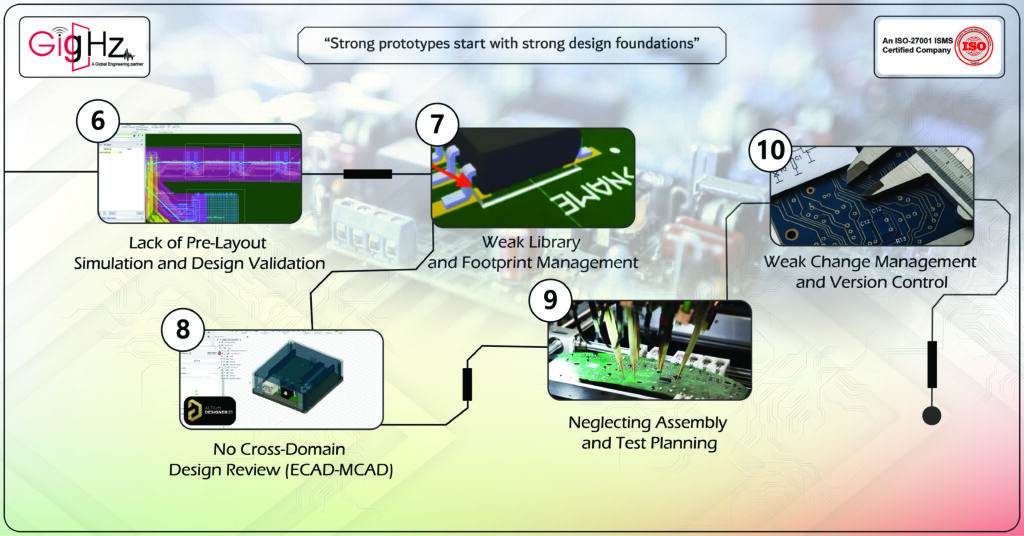
6. Lack of Pre-Layout Simulation and Design Validation
Students often fabricate boards without running SI (Signal Integrity) or PI (Power Integrity) simulations.
Result:
Crosstalk, overshoot, ringing, and timing violations that make the circuit unreliable.
Professional Fix:
Run pre-layout simulations for:
- Critical nets (e.g., high-speed clocks, differential pairs)
- Transmission line impedance
- Power distribution noise
Tools like HyperLynx, Ansys SIwave, or even free tools (e.g., QUCS, LTspice) can expose these problems early.
7. Weak Library and Footprint Management
Footprint mismatches, pin swaps, or incorrect pad sizes are major re-spin causes.
Common Issues:
- Inconsistent symbol naming
- No IPC footprint compliance
- Missing 3D models for mechanical validation
Professional Fix:
Create or source footprints from verified libraries (IPC-7351 compliant).
Maintain a centralized version-controlled library shared across all design members.
8. No Cross-Domain Design Review (ECAD-MCAD)
Without early coordination between electronics and mechanical teams, student startups face fitment and enclosure integration issues.
Examples:
- Connector misalignment with enclosure ports
- Mounting holes overlapping components
- PCB thickness mismatch in CAD model
Professional Fix:
Perform ECAD-MCAD integration checks using STEP exports.
Use co-design tools (like Altium CoDesigner or Fusion 360) to detect mechanical clashes early.
9. Neglecting Assembly and Test Planning
Students rarely plan Design for Assembly (DFA) or Design for Test (DFT) until after the PCB is made.
Consequences:
- No test pads for debugging
- Manual soldering of fine-pitch components
- Difficulty probing critical nets
Professional Fix:
Design with testing in mind — add test points, consider JTAG or boundary-scan access, and plan for fixture-based testing from the start.
10. Weak Change Management and Version Control
Team members often overwrite each other’s files or lose revision history due to poor file management.
Professional Fix:
Use Git-based version control or PLM systems (like Altium 365 or Fusion Manage).
Maintain structured folders for schematic, layout, BOM, and fabrication files.
Document every major design iteration.
Bottom Line
Student-led hardware startups companies often have innovation—but not process discipline.
By treating every prototype like a production design, your team will:
- Reduce design re-spins
- Shorten prototype cycles
- Build credibility with investors and incubators
If your team needs help with simulation, manufacturability review, or DFM validation, our engineering experts can assist — from schematic validation to EMC-safe layout design.
Explore our PCB Design and Simulation Services to fast-track your next prototype.
Book a Call. Schedule a Free Consultation now https://calendly.com/gighz/30min
Stuck in a loop of challenges? Always pick smart solution that works
Have you faced costly rework because 2D drawings skipped in MCAD workflows?
Effective way to prevent MCAD documentation errors recalls?
Please answer both poll questions before submitting.
Thank you for your response! 😊
Latest Post
Get Customized Engineering CAD Design Service

Book a Free Consultation Call
Partner with Gighz and bring your most innovative design concepts to life. Our engineering cad services accelerate development so you can focus on your big vision.