
In a startup, time and money move faster than anything else. You have a great product idea, a small team, and a strict deadline but one part of the journey needs the right focus to stay on track — PCB design.
Many founders underestimate it at first. They assume it’s just about placing components and sending files for fabrication.
But soon, small design errors turn into long delays. A missing constraint, a wrong footprint, a poor layout decision — each one adds another round of fixes and more waiting.
It’s not that startups design badly — it’s that they often design without enough visibility.
Reducing PCB cost and time isn’t about rushing or compromising quality. It’s about designing with clarity, verifying decisions early, and building a workflow that avoids rework.
Let’s break down how that’s done.
1. Understand Where the Real Cost Comes From
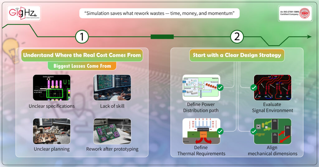
PCB cost isn’t just about fabrication or components. The biggest losses come from what you don’t see — unclear specifications, missing documentation, and rework after prototyping.
Every time a design is corrected after production, it means double spending: once for the board that failed, and again for the one that replaces it.
The time between those two also costs — your testing, software, and marketing plans all get delayed.
These delays are rarely due to lack of skill. They come from unclear planning. When the design requirements are vague, engineers make assumptions.
Later, those assumptions show up as design mismatches or performance problems.
So before you try to reduce cost through cheaper parts or faster fabrication, look at where time actually goes. You’ll often find that the real expense comes from uncertainty.
And once you fix that, everything else starts to move smoother.
2. Start with a Clear Design Strategy
A robust PCB design begins with a clear understanding of the board’s electrical, thermal, and mechanical requirements.
Before opening your layout tool, define the power distribution path — current flow, voltage limits, and return paths.
These parameters directly determine trace width, copper thickness, and via count.
If trace dimensions don’t support the expected current density, it leads to resistive heating, voltage drop, and long-term reliability issues.
Next, evaluate your signal environment. High-speed or high-frequency signals must be treated as transmission lines, which means impedance control is non-negotiable.
Plan your stack-up, dielectric constant (Dk), and trace geometry carefully. The moment fabrication starts, these parameters become fixed, and signal integrity issues can’t be corrected later.
On the thermal side, estimate component power dissipation and define proper heat-spreading paths using copper pours, thermal vias, or dedicated heat sinks.
Stable thermal design prevents localized hotspots and extends component life.
Mechanically, fix the board outline, mounting holes, and connector placement early in alignment with the enclosure and mechanical CAD model.
Late changes to these parameters usually require re-routing and can break impedance or clearance constraints.
When all these design constraints are clear from the start, your first layout iteration becomes stable, compliant, and nearly production-ready — not a trial version.
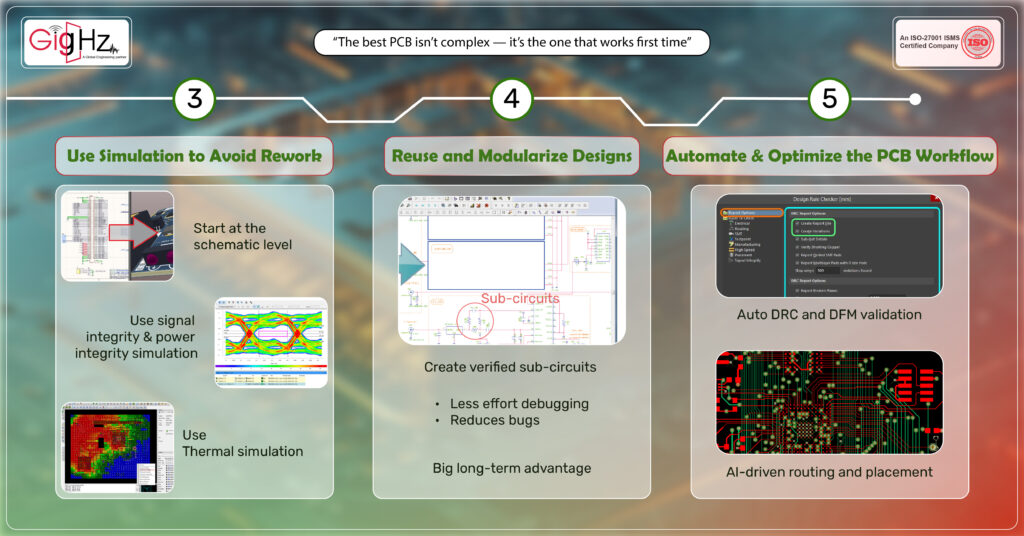
3. Use Simulation to Avoid Rework
Many startups skip simulation, assuming it’s complex or time-consuming. In reality, it’s the fastest way to prevent costly redesigns and schedule slips.
Every failed prototype adds up — not just in fabrication and assembly cost, but also in lost development time.
Simulation helps you predict how the board will behave before you manufacture it, giving visibility into electrical, thermal, and signal performance.
Start at the schematic level. Validate voltage stability, current flow, and power ripple across the circuit.
Identify overstressed components or unstable regulator loops early. After layout, use signal integrity (SI) simulation to observe real-world effects like reflections, ringing, and crosstalk.
You’ll see how trace impedance, termination, and length matching affect waveform quality.
Then move to power integrity (PI) simulation. Verify voltage drop across planes, decoupling capacitor effectiveness, and PDN resonance.
This ensures every IC sees a clean and stable supply under load.
Finally, use thermal simulation to map temperature gradients — finding hotspots, insufficient copper areas, or poor heat via placement before they become physical failures.
Modern ECAD tools like Altium Designer, Cadence OrCAD/Allegro, Siemens PADS, and KiCad make simulation fast and accessible.
They include built-in features for signal integrity, power integrity, and basic thermal analysis, allowing you to visualize how the board performs before fabrication.
A few hours of simulation in these platforms can replace weeks of troubleshooting and rebuilds. For startups, that’s not just cost saving — it’s design momentum.
4. Reuse and Modularize Designs
Not every circuit has to be created from scratch. Building reusable design blocks is one of the most effective long-term strategies for startups.
Create verified sub-circuits — like power supply modules, communication interfaces, or sensor input sections — that can be dropped into new designs with minimal change.
Each verified block becomes a trusted asset.
This approach shortens development time dramatically. You spend less effort debugging, because you already know those circuits work.
It also creates design consistency across projects, making maintenance and updates easier in the future.
Over time, your internal library becomes a quiet strength. The more you reuse, the faster and safer your next project moves.
5. Automate and Optimize the PCB Workflow
For startups and university spin-offs, speed and precision decide survival.
PCB automation replaces slow, manual steps with smart, rule-based workflows that save time and reduce cost across the design cycle.
It begins with automated library management, where tools create component symbols, footprints, and 3D models directly from datasheets or IPC standards.
Centralized cloud libraries maintain version control and eliminate pin or footprint mismatches — cutting library creation time by up to 70%.
Then comes auto DRC and DFM validation, where rule-based checks instantly flag spacing, trace, or via errors while ensuring manufacturability.
This reduces review time by nearly 30% and shortens design iterations from several rounds to just one or two.
With AI-driven routing and placement, components are automatically positioned for performance and efficiency.
Traces are optimized for signal integrity, reducing layout time by almost half — ideal for rapid MVP and prototype builds.
Automated BOM and sourcing integration links directly with supplier databases like Digi-Key or Mouser, enabling real-time part selection, cost comparison, and alternate sourcing — preventing redesign delays and keeping projects on schedule.
Finally, simulation-driven automation validates electrical and thermal behavior before fabrication.
Automated SI, PI, and thermal checks ensure first-time-right boards and minimize prototype re-spins.
Bottom Line
A startup’s biggest strength is agility — the ability to move quickly and adapt. But speed without structure only creates rework.
Reducing PCB design cost and time is not about skipping steps; it’s about doing each step with awareness.
When you plan clearly, validate through simulation, and collaborate early, you minimize risk and build confidence in your design process.
The reward is not just a lower bill or a shorter schedule. It’s a product that works the first time you power it up.
It’s the quiet relief of knowing your design is stable, manufacturable, and ready to grow with your company.
In the end, the smartest PCB design isn’t the one that looks the most complex — it’s the one that moves from concept to production with the least resistance.
Design smart, design disciplined, and let every decision bring you closer to launch — not back to redesign.
Book a call. Schedule a Free Consultation now https://calendly.com/gighz/30min
Stuck in a loop of challenges? Always pick smart solution that works
Have you faced costly rework because 2D drawings skipped in MCAD workflows?
Effective way to prevent MCAD documentation errors recalls?
Please answer both poll questions before submitting.
Thank you for your response! 😊
Latest Post
Get Customized Engineering CAD Design Service

Book a Free Consultation Call
Partner with Gighz and bring your most innovative design concepts to life. Our engineering cad services accelerate development so you can focus on your big vision.