Why Most PCB Designs Fail in First Manufacturing and How to Prevent
- Posted On:
- October 9, 2025
- Category:
- Ecad
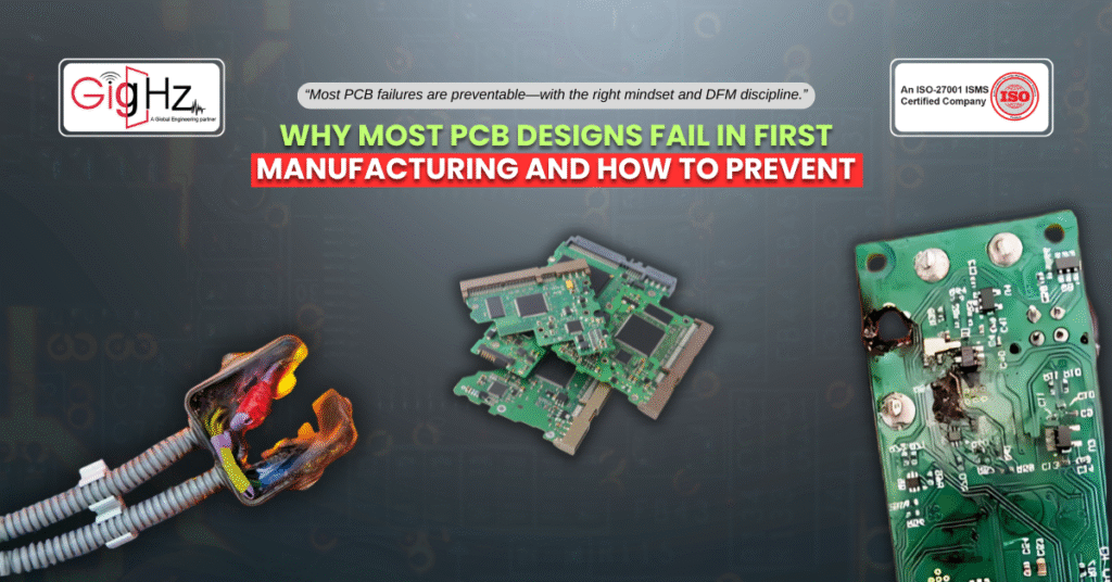
Nearly 70% of new PCB designs fail in their very first manufacturing run.
Yes, engineers invest weeks of effort into schematics and layouts but only to watch the first prototypes come back with issues like:
- Short circuits
- Open enclosures
- Assembly issues, or signal problems
And while people often blame complexity or tight deadlines, the real issue lies in ignoring DFM in PCB design.
Likewise, the gap between what’s possible in ECAD and what’s manufacturable on a real production line is where most first-pass failures occur. So, the good news?
Well, these failures are predictable and preventable but only if you approach design with the right mindset and discipline.
So, let’s break down the seven most common failure points in PCB and the steps you can take to ensure your next board doesn’t fall into the same trap.
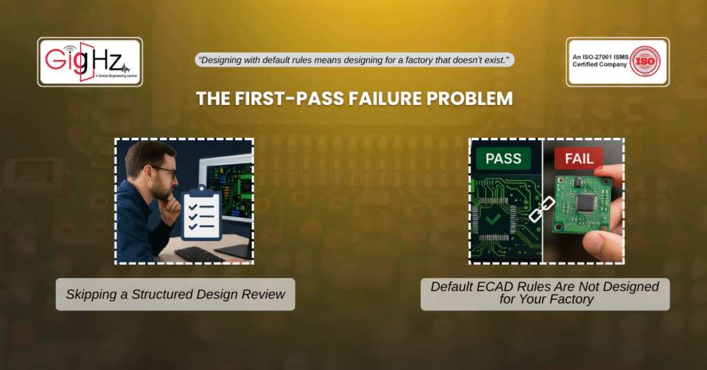
1. Skipping a Structured Design Review - PCB Design Fail
So, one of the easiest ways to prevent PCB design errors is also one of the most overlooked ones nowadays. As the review process begins, many teams rely solely on automated checks, but a well-run peer review can catch issues tools simply miss.
Evidently, a proper PCB design review checklist should include:
- Footprint-to-datasheet verification
- Schematic-to-layout netlist checks
- Review of power and ground distribution
- Assembly clearances, thermal reliefs, and test point accessibility
Likewise, a checklist-driven review acts as a safety net. Without it, small ECAD design mistakes can sneak through and cause catastrophic production failures.
2. Default ECAD Rules Are Not Designed for Your Factory
Besides, most engineers trust their tool’s default design constraints. But what works in ECAD doesn’t always work on the fab floor.
Common issues that arise from default DRC settings:
- Drill-to-copper clearances too tight for your vendor’s capabilities
- Inadequate annular ring sizing for reliable via plating
- Copper-to-edge violations that result in shorts or cut traces
So, always align your constraints with your specific manufacturer’s capabilities. Otherwise, you’re designing for an imaginary factory.
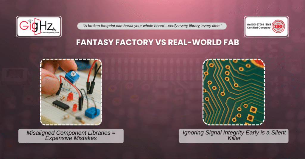
3. Misaligned Component Libraries = Expensive Mistakes
Also, incorrect footprints are one of the most expensive errors and they’re shockingly common. Apparently, just one incorrect pinout or pad dimension can destroy an entire batch of boards.
Make sure your library QA process includes:
- Pinout verification against the datasheet
- Pad sizing and solder mask alignment checks
- 3D model and silkscreen placement accuracy
- Version control for shared libraries
- Use IPC-compliant automated tools to validate component footprints and pin configurations.
A trusted library is a design asset.
An unchecked one is a liability waiting to happen.
4. Ignoring Signal Integrity Early is a Silent Killer
Also, high-speed signals demand more than just neat routing and they require deliberate planning from the start. And yet, many teams wait until post-layout to think about signal integrity.
Likewise, critical signal integrity considerations to catch early:
- Differential pair tuning and spacing
- Controlled impedance setup on high-speed lines
- Avoiding stubs and long trace lengths
- Via transitions and return path continuity
Running pre-layout simulations and embedding constraints directly into your tool can eliminate entire classes of failures before routing even begins.
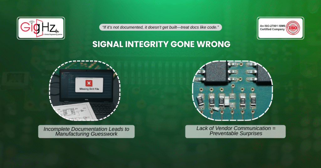
5. Incomplete Documentation Leads to Manufacturing Guesswork
Even the most beautifully routed PCB is useless without proper documentation. A missing drill file or vague assembly note can derail the entire build.
Ensure your documentation package includes:
- Gerbers and drill files
- Pick-and-place and centroid data
- Detailed assembly drawings with part orientation
- Fabrication notes and stack-up details
- Clear versioning and revision control
Also, documentation isn’t an afterthought as it’s a deliverable.
6. Lack of Vendor Communication = Preventable Surprises
Finally, your fabrication house isn’t just a vendor as they’re part of your success. So, failing to engage with them before tape-out is a gamble.
Besides, preventable misalignments include:
- Specifying microvias when the shop only does through-hole
- Choosing exotic copper weights or materials without checking availability
- Assuming RoHS compliance or lead-free profiles without confirmation
Putting It All Together: The “Prevention Framework”
Now, here’s a simple three-step framework:
- Standardize Reviews: Use a PCB design review checklist on every project, no exceptions.
- Customize Rules: Align ECAD DRC settings with your manufacturer’s exact capabilities.
- Validate Early: Run signal integrity checks, library audits, and documentation reviews before tape-out.
Therefore, by focusing on prevention instead of firefighting, you’ll significantly reduce first-pass risks.
Bottom Line
Summing up, the reality is that most boards don’t fail because of advanced physics or out of the box complexities.
Accordingly, they fail because of preventable ECAD design mistakes, overlooked PCB design review checklist steps, and common DRC issues in PCB layout.
Also, when you embed prevention into your process, you stop treating re-spins as inevitable and start treating them as avoidable.
That’s how you consistently prevent PCB design errors and achieve first-pass success.
Similarly, at Gighz, we’ve seen teams transform from three or four failed first runs to hitting >90% first-pass success.
The difference wasn’t better luck—it was a better process.
Therefore, act now, and Prevent obsolescence from becoming your next roadblock—act before it strikes.
Contact us right away at info@gighz.net for a free consultation!
Follow us at Linkedin https://www.linkedin.com/company/3483128/admin/dashboard/
Stuck in a loop of challenges? Always pick smart solution that works
Have you faced costly rework because 2D drawings skipped in MCAD workflows?
Effective way to prevent MCAD documentation errors recalls?
Please answer both poll questions before submitting.
Thank you for your response! 😊
Latest Post
Get Customized Engineering CAD Design Service

Book a Free Consultation Call
Partner with Gighz and bring your most innovative design concepts to life. Our engineering cad services accelerate development so you can focus on your big vision.