5 Tips to Overcome emerging Miniaturization Challenges in PCB Design
- Posted On:
- October 1, 2024
- Category:
- Ecad

Miniaturization Challenges
You may have faced a situation of losing your phone or a key that made you completely frustrating.
This kind of situations usually occurs when you are in a hurry that you can’t be late for.
In such cases, a smartwatch can really help you out.
Most of the smartwatch holds a feature ‘find phone’ that you can connect your phone or any other device with the watch and is able to make a ring through your watch.
If you lost your phone, just press a few buttons on your watch that makes you locate the phone within seconds.
Even though there are many smartwatches from different brands available, some people think they’re useless or a waste of money.
This opinion usually comes from not fully understanding what a smartwatch can do and its benefits.
So, how does it tracks?
It’s through the Printed Circuit Board (PCB) fitted inside the watch.
The biggest challenge in designing these PCBs is miniaturization.
Miniaturization in smartwatch design is tough because fitting many parts into a tiny space is challenging.
It makes managing heat, keeping signals clear, and distributing power harder.
Plus, making and assembling these small parts precisely can increase costs and the chance of errors.
Let’s dig into the 5 tips to overcome these challenges!
5 Tips To Overcome emerging Miniaturization Challenges In PCB Design

As smartwatches evolve into increasingly sophisticated devices, the challenge of miniaturizing their printed circuit boards (PCBs) becomes more pressing.
Designing PCBs for smartwatches involves not only fitting a multitude of functionalities into a compact space but also ensuring that the design meets performance, thermal, and manufacturability standards.
1. Component Placement and Integration in PCB Design
Challenge: Space Constraints and Component Size
The compact size of smartwatches means that the PCB must be designed to maximize available space while integrating various components such as sensors, processors, and communication modules. The limited area poses significant challenges in placing and interconnecting these components without causing layout congestion or performance degradation.
To address these space constraints, designers can employ several strategies:
Use miniaturized components like 0201 (0.6mm x 0.3mm) packages and System-in-Package (SiP) solutions. These components help conserve space by integrating multiple functions into single packages, thus reducing the overall footprint.
Implement multi-layer PCBs (up to 12 layers) to manage space efficiently. By segregating signal, power, and ground planes across different layers, designers can simplify routing and avoid overcrowding on a single layer.
- Signal Integrity and Electromagnetic Interference (EMI)
Challenge: Signal Degradation and EMI
With the increasing density of components on the PCB, maintaining signal integrity becomes challenging. High-speed signals and closely packed traces are susceptible to crosstalk and signal degradation. Additionally, dense designs can exacerbate electromagnetic interference (EMI), which can impact device performance and nearby electronics.
Effective signal integrity and EMI management can be achieved through the following techniques:
Design traces with controlled impedance, such as 50Ω for single-ended signals and 100Ω for differential pairs. Utilize impedance calculators and simulation tools to ensure accurate impedance matching.
Incorporate EMI shielding techniques like metal shielding layers and filter capacitors (0.1µF) to reduce interference. Place sensitive traces away from high-frequency components and employ ground planes to shield critical signal paths.
3. Thermal Management
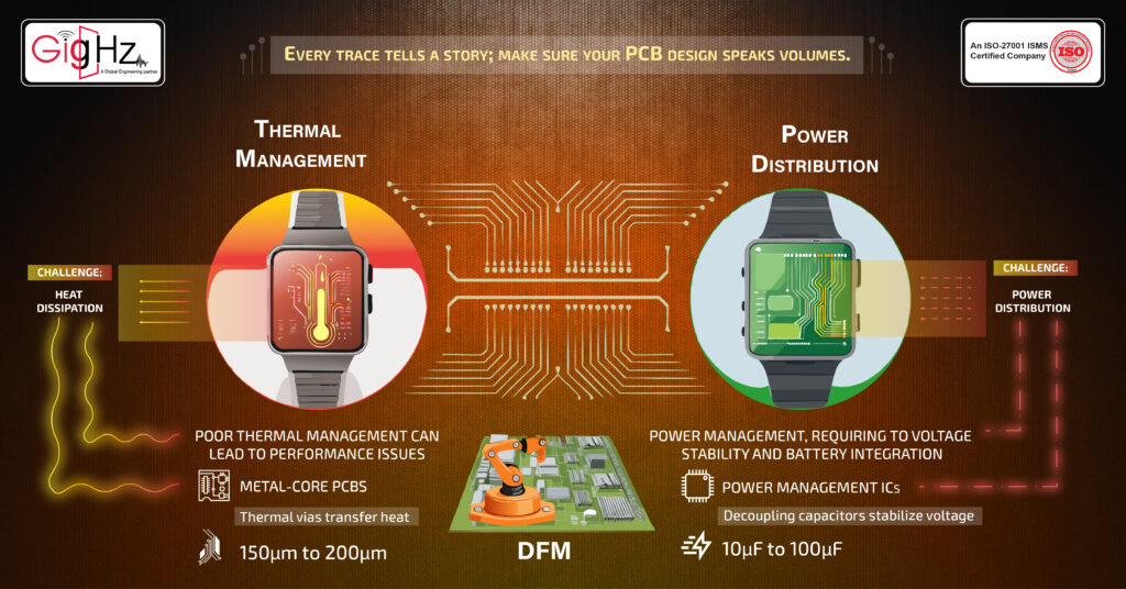
Challenge: Heat Dissipation
Miniaturized PCBs with high-performance components can generate significant heat, which must be effectively managed to prevent overheating and ensure device reliability. Poor thermal management can lead to performance issues and reduced lifespan of the smartwatch.
To address thermal challenges,
Use thermal vias with diameters of 150µm to 200µm to transfer heat away from high-power components to heat sinks or outer layers. Integrating small heat sinks or thermal pads can also help dissipate heat more effectively.
Opt for substrates with high thermal conductivity, such as ceramic or metal-core PCBs, to enhance heat dissipation and manage thermal load more efficiently.
- Power Distribution and Management
Challenge: Power Integrity and Battery Integration
Efficient power distribution is critical for smartwatches, which have varying power requirements for different components. The compact design of smartwatches further complicates power management, requiring careful attention to voltage stability and battery integration.
To ensure reliable power distribution, consider the following:
Implement dedicated power and ground planes with a minimum thickness of 1 oz/ft² to reduce impedance and voltage drops. This helps maintain stable power delivery across the PCB.
Integrate Power Management ICs (PMICs) to handle multiple power rails efficiently. Place decoupling capacitors (10µF to 100µF) close to IC power pins to stabilize voltage levels and minimize noise.
- Design for Manufacturability and Assembly
Challenge: Manufacturing Precision and Assembly Complexity
Miniaturized designs with small components demand precise manufacturing and assembly processes. Errors or defects in fabrication and assembly can lead to functionality issues and increased production costs.
To ensure manufacturability and assembly efficiency, implement the following practices:
Follow design for manufacturability (DFM) rules, including minimum trace widths (typically 4 mils or 0.1mm) and spacing requirements. Align design features with the capabilities of PCB manufacturers and assembly services.
Conduct thorough prototyping and testing to identify and resolve potential issues early. Utilize automated optical inspection (AOI) and X-ray inspection to ensure accurate component placement and solder joint quality.
Role of PCB in Smartwatch Functionality
Impact of PCB Design on Smartwatch Performance
The performance of a smartwatch is heavily influenced by the quality and design of its PCB. Effective PCB design ensures:
- Reliability: Minimizing signal interference and ensuring robust power delivery contribute to the overall reliability of the smartwatch.
- Functionality: Proper integration of components and effective thermal management enhance the smartwatch’s performance and user experience.
- Battery Life: Efficient power management through well-designed PCBs extends battery life, a crucial aspect for wearable devices.
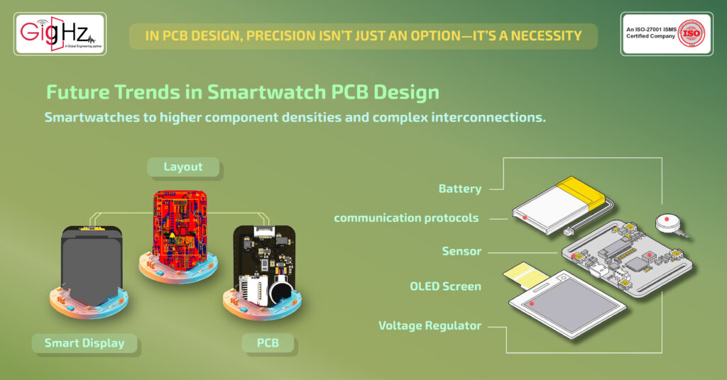
Future Trends in Smartwatch PCB Design
As smartwatches continue to evolve, PCB design will need to keep pace with emerging technologies and trends:
- Increased Integration: Future smartwatches may incorporate even more functionalities, requiring advanced PCB designs that support higher component densities and complex interconnections.
- Wearable Electronics: The integration of new sensor technologies and advanced communication protocols will drive further innovation in PCB design for wearables.
Final Thoughts
The pcb layout is a critical aspect of circuit board design that directly impacts the functionality and reliability of electronic devices. As pcb designers navigate the design process, they must prioritize signal integrity issues and ensure electromagnetic compatibility to mitigate common problems faced in the electronics industry. This is especially true for medical devices, where compliance with strict regulations is essential. The emergence of HDI technology and BGA packages introduces both opportunities and challenges for pcb development, highlighting the need for automation and interactive routing to optimize designs.
As engineers strive to meet the demands of increasingly complex pcbs, they must consider wiring, ground and power planes, and the width and spacing of circuitry. Understanding trends and challenges in the industry allows for innovative problems and solutions to emerge. By addressing major challenges such as improper layout and ensuring compatibility, designers must consider all aspects of the pcb design process to create pcbs that meet the high standards required for modern applications.
Book a Time to Discuss Your Needs! https://calendly.com/gighz/30min
Table of Contents
Latest Post
Get Customized Engineering CAD Design Service

Book a Free Consultation Call
Partner with Gighz and bring your most innovative design concepts to life. Our engineering cad services accelerate development so you can focus on your big vision.