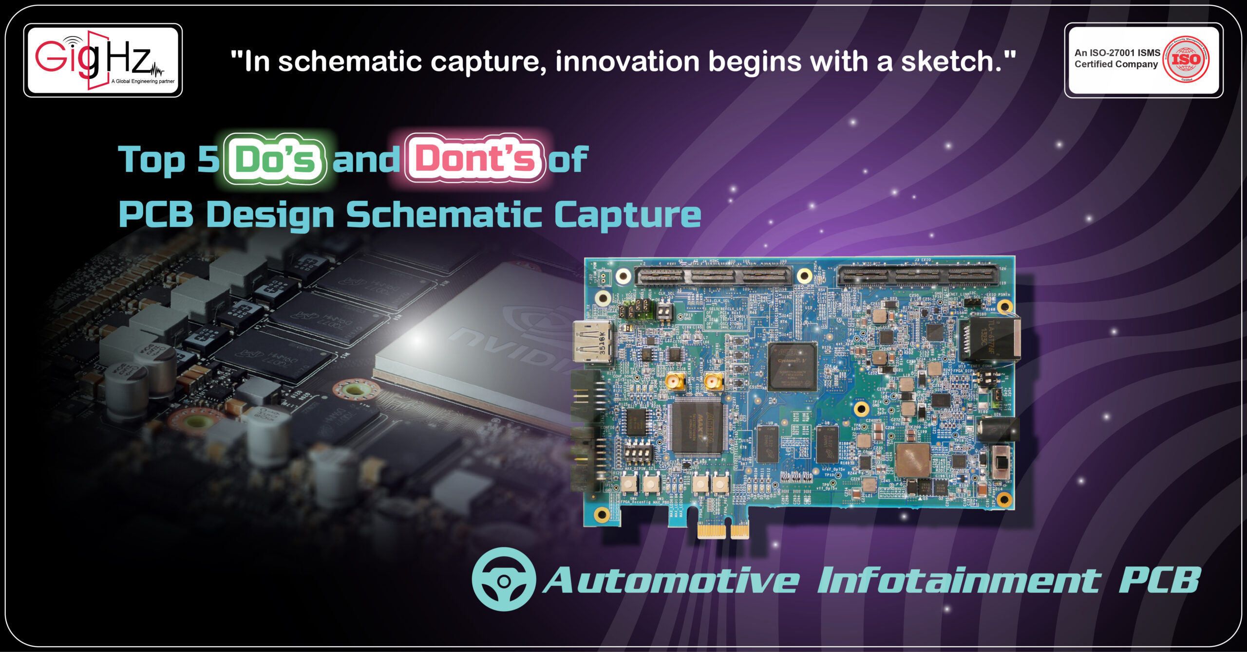
Top 5 Do’s and Dont’s of PCB Design Schematic Capture
Hey there!
Welcome to Everyone, So, when it comes to PCB design, the schematic capture process is super important for a few reasons. First off, it’s like the foundation for designing the electronic circuitry within the PCB design software. This part allows us to see how all the electrical connections will work in the circuit board design.
Hey there!
Welcome to Everyone,
So, when it comes to PCB design, the schematic capture process is super important for a few reasons.
First off, it’s like the foundation for designing the electronic circuitry within the PCB design software.
This part allows us to see how all the electrical connections will work in the circuit board design.
Category :
Published Date :
March 28, 2024
Category :
Published Date :
March 28, 2024
Category :
Published Date :
March 28, 2024
The cool thing is that the info we put into the schematic drawing is what we use to finish up the PCB layout.
It ensures that we place the components in the right spots and connect them properly to make sure everything works as intended.
Another neat aspect is that schematic capture helps engineers move on to simulating or laying out the actual board.
This way, we can visualize and test how the circuit will behave before actually building it.
By drawing the schematic and detailing the size and type of components, we create a clear plan for the rest of the PCB design process.
This whole approach ensures that the PCB layout accurately matches the intended circuit design, making production more efficient and the performance reliable.
Cool, right?
Let’s dig in detail, what we have done for Infotainment PCB design layout Board Schematic Capture,
Understanding Schematic Capture in PCB Layout
Schematic capture is the process of creating a visual representation of an electronic circuit using specialized software.
It’s like drawing a map that shows how different electronic components, such as resistors, capacitors, and integrated circuits, are connected to each other to form a complete circuit.
This visual representation, known as a schematic diagram, helps us to understand the inner workings of the circuit and is essential for tasks like simulation, testing, and PCB (Printed Circuit Board) layout.
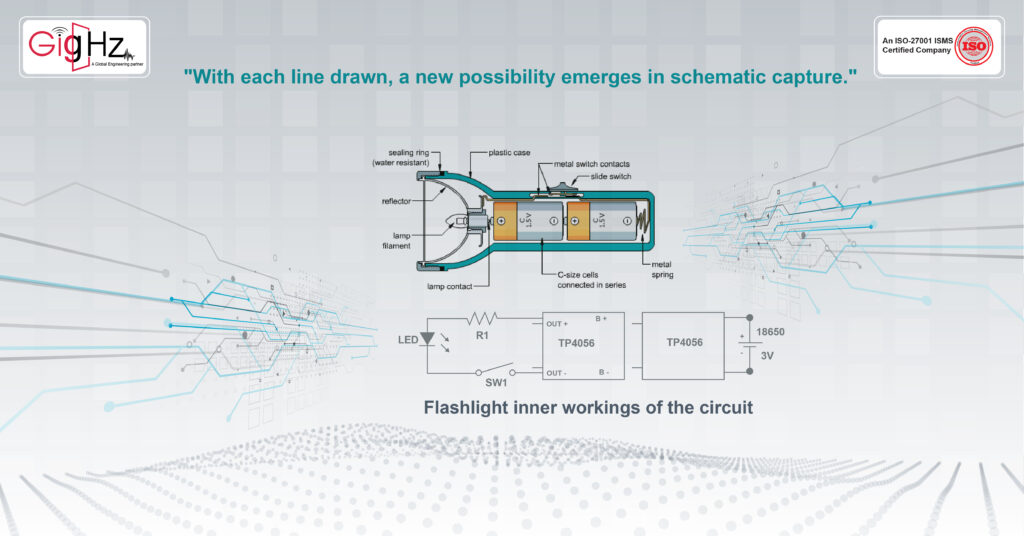
For example, if you imagine a simple flashlight circuit, the schematic capture would involve using symbols to represent the battery, the switch, the bulb, and the connecting wires.
By visually mapping out how these components are interconnected, the schematic provides a clear understanding of how the flashlight circuit functions.
Core Concepts in Schematic Entry we follow
The basic principles followed for schematic capture included in the pcb design,
Symbol Standards:
Utilizing standardized symbols for components, ensuring consistency and universal understanding across different circuits.
Logical Connectivity:
Accurately representing the flow of signals through the circuit, depicting how components are interconnected and how the circuit functions as a whole.
Conciseness:
Presenting the circuit in a clear and uncluttered manner, avoiding unnecessary complexity to enhance readability and comprehension.
Documentation:
Including detailed annotations and labels to document the purpose and characteristics of each component and connection within the circuit.
Standards Compliance:
Adhering to industry standards to ensure compatibility with various tools and processes involved in electronic design and manufacturing.
Rules of thumb for schematic capture in PCB Layout we use
Throughout the process of schematic capture, you will engage with a graphical interface, utilizing it to place component models in drawings and connect them with wires.
To optimize your efficiency and enhance the readability of your schematic sheets, there exist several fundamental practices that can save you time and streamline the interpretation of the schematics.
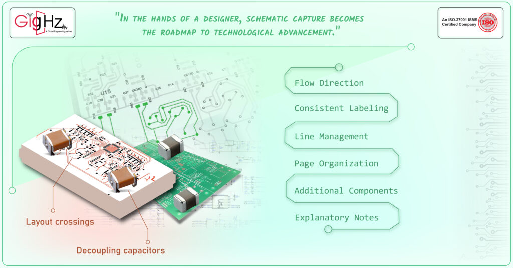
Flow Direction:
Initially, we arrange components so that the signal flow goes from left to right (input to output) and power supply flows from top to bottom.
This ensures clarity in understanding how signals and power move through the circuit.
Consistent Labeling:
We use a uniform naming convention for all labels to make it easy for readers to understand and identify potential issues at a glance.
This helps in debugging the circuit design before layout and manufacturing.
Line Management:
Then we minimize wire crossings or convergence to avoid confusion.
If wires need to cross, we make it clear to the read.
We limit the convergence of lines to a maximum of three to prevent misunderstanding.
Page Organization:
If the schematic spans multiple pages, separate components so that each page contains complete functional blocks.
We ensure clear identification of connections between pages for better understanding.
Inclusion of Additional Components:
We always remember to include additional parts like decoupling capacitors and line filters in the schematic. Forgetting these can lead to invalid simulation results and non-functional end products.
Explanatory Notes:
We also add explanatory notes wherever needed to clarify any unclear aspects of the schematic. This helps in understanding the design decisions later and fosters clear communication within the team.
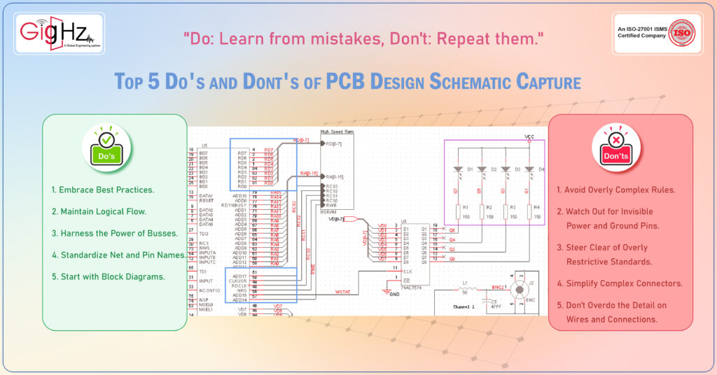
Top 5 Do's and Dont's of PCB Design Schematic Capture
When it comes to capturing schematics for PCB design, there are some key do’s and don’ts that can make a significant difference in the quality and usability of your designs.
Let’s dive into these insights to ensure that your schematic capture process is not only technically sound but also practical and effective.
The Do’s of Schematic Capture:
1. Embrace Best Practices
When diving into schematic capture, it’s crucial to embrace and follow best practices. These practices are the guiding principles that ensure you’re heading in the right direction from the get-go.
They help bring consistency, clarity, and efficiency to your designs, ultimately resulting in higher-quality schematics.
2. Maintain Logical Flow
Ever heard of the phrase “order out of chaos”?
Well, that’s precisely what you should aim for when arranging your schematics.
Keep things organized by placing higher voltages at the top, lower voltages at the bottom, and maintaining a logical flow from left to right.
This simple practice can significantly enhance the readability and usability of your schematics.
3. Harness the Power of Busses
Busses are like the organizational superheroes of schematics.
Wherever possible, utilize busses to streamline your design and improve its overall readability.
They’re fantastic for tidying up connections and making your schematics more comprehensible at a glance.
4. Standardize Net and Pin Names
Consistency is key, especially when it comes to net and pin names.
Using all caps for these elements aligns with industry conventions and datasheet standards, making it easier for anyone to understand and work with your schematics.
5. Start with Block Diagrams
Before delving into the nitty-gritty details of schematic capture, consider starting with a block diagram.
This big-picture view allows you to map out the overall design flow, providing a clear roadmap for the subsequent detailed schematic capture process.
The Dont’s of Schematic Capture:
1. Avoid Overly Complex Rules
While rules are essential, they shouldn’t come at the cost of readability.
If a particular rule makes your design overly complex and compromises its clarity, it’s best to reevaluate its necessity.
2. Watch Out for Invisible Power and Ground Pins
In modern designs, invisible power and ground pins can be sneaky culprits that lead to unexpected connections during the layout phase.
Stay vigilant and ensure that these critical elements remain visible and properly accounted for in your schematics.
3. Steer Clear of Overly Restrictive Standards
Standards are there to guide us, not hinder us.
Overly restrictive standards can stifle creativity and practicality in schematic design.
Remember to balance adherence to standards with the practical needs of your specific design.
4. Simplify Complex Connectors
Connectors are vital components, but they shouldn’t look like something out of a complex puzzle.
Keep them clear and comprehensible to avoid confusion down the line during high-speed PCB layout and assembly.
5. Don’t Overdo the Detail on Wires and Connections
While attention to detail is crucial, there’s such a thing as too much detail.
Avoid cluttering your schematics with unnecessarily intricate wire representations, as this can obscure the overall readability of the design.
By keeping these do’s and don’ts in mind throughout your schematic capture process, you’re setting yourself up for success in creating high-quality and usable circuit board schematics.
Our Notable Upgrade: Engineering as a Service (EaaS)
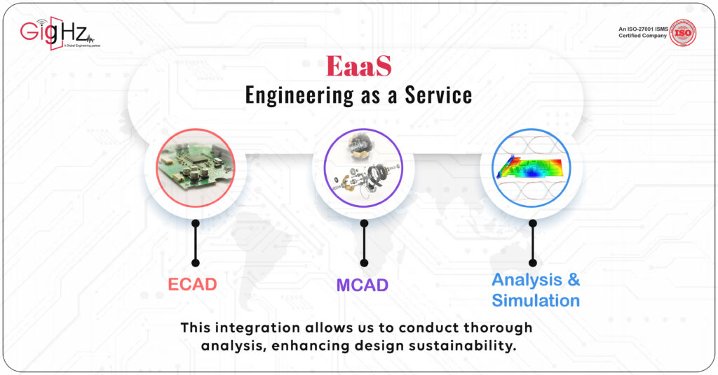
Absolutely! Amid the growing prevalence of intricate engineering challenges, our Engineering as a Service (EaaS) offering is undeniably enhancing its impact.
We are harnessing the collective capabilities of ECAD, MCAD, and Analysis & Simulation, positioning us as leaders in the industry.
What’s especially thrilling is our provision of an all-encompassing solution that spans the entirety of the engineering workflow.
It’s genuinely exhilarating!
Conclusion
After completing our schematics and preparing for PCB layout phase, modern design tools offer the capability to automate the transition to a physical design.
Instead of the traditional method involving exporting a netlist from the schematic editor and then re-importing it into a PCB editor, advanced tools can streamline this process by directly importing your component data into a new PCB layout.
Nevertheless, it is crucial to conduct a thorough review of each circuit diagram in our schematic sheets before proceeding with the board manufacturing process.
While most software packages provide rule check features to detect potential errors such as opens and shorts, these functionalities should complement, not replace, a comprehensive manual schematic design review.
Schedule a Call. Book a Free Consultation now. https://calendly.com/gighz/30min
To discover our Specialities. Visit our Services Page. https://gighz.net/services/