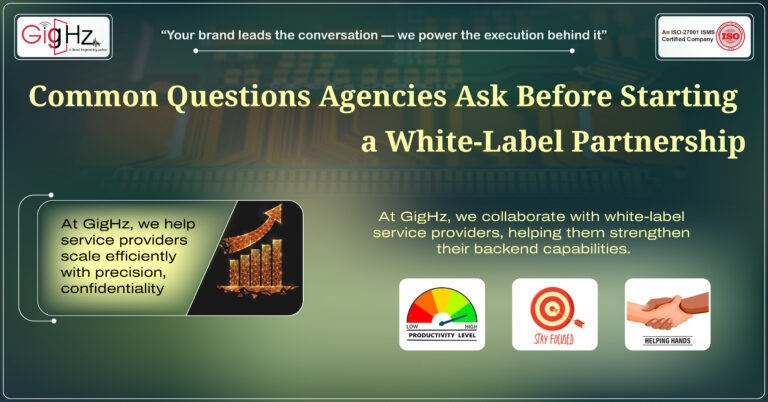
In today’s fast-paced hardware market, white-label Partnership face increasing pressure to deliver complete product solutions — from...
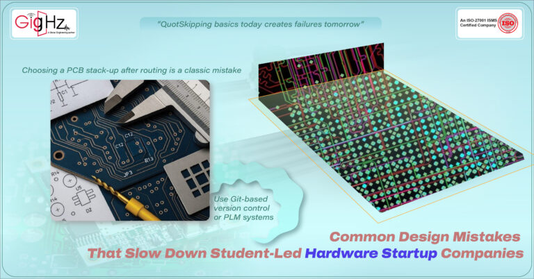
Every student hardware team knows the excitement of building a new idea.
You sketch the system, design the PCB, send the files to fabrication...
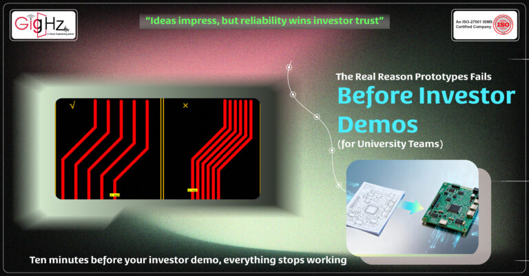
Ten minutes before your investor demo, everything stops working. Frustratingly, this happens again and again, even to the most promising...
Every university PCB project starts with a working prototype — the LEDs blink, power flows, and the board performs as expected.
But...
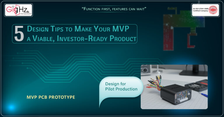
Every startup begins with an idea.But turning that idea into something an investor can see, touch, and believe in — that’s the real...

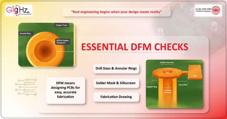
Every circuit board looks perfect when it’s new — clean traces, bright copper, solid solder joints.
But once power flows through it,...