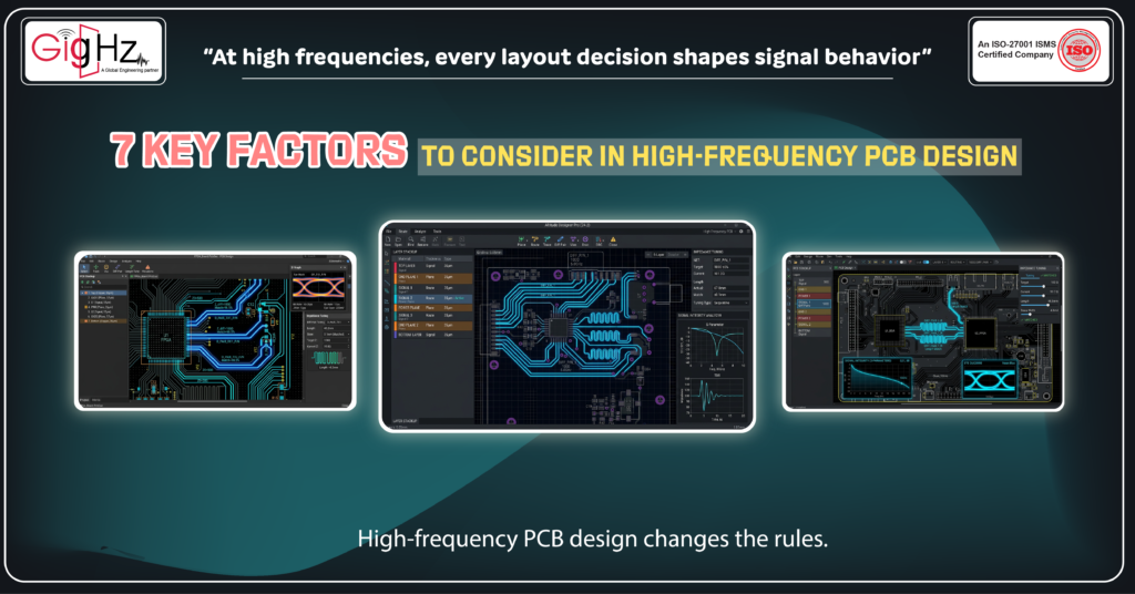
High-frequency PCB design changes the rules.
At low speeds, traces behave like simple wires.
At high speeds, they behave like signal highways.
Small layout choices suddenly start creating big problems.
A slightly longer trace.
A broken ground reference.
A poorly placed decoupling capacitor.
And suddenly the board shows issues like:
Random data errors
Noise spikes in RF circuits
Timing instability in high-speed interfaces
What’s surprising?
Most of these problems are not caused by the schematic.
They usually come from PCB layout decisions made early in the design stage.
As signal speeds increase, the board itself becomes part of the electrical system.
Traces, planes, and component placement start influencing how signals behave.
That’s why careful layout planning from the beginning is critical.
Below are 7 key factors that help engineers design stable, reliable boards for high-speed applications.
7 Key Factors That Influence High-Frequency PCB Performance
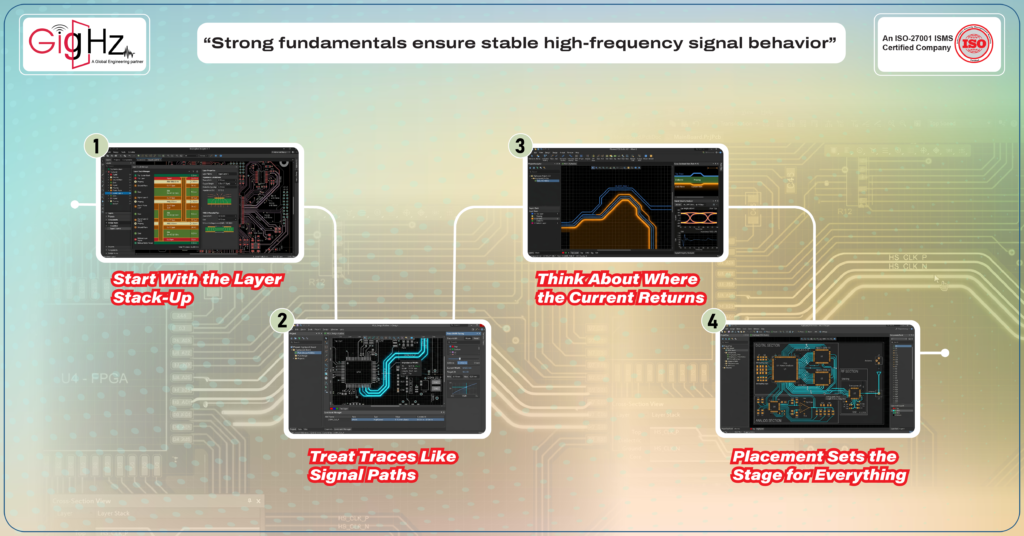
1. Start With the Layer Stack-Up
Think of the layer stack-up as the structural backbone of the PCB. It determines how signals interact with reference planes and how impedance is controlled.
A good stack-up helps signals travel cleanly and predictably.
Key practices:
- Place ground planes close to signal layers
• Maintain controlled impedance paths
• Avoid unnecessary layer changes later in the design
• Work with manufacturers early for stack-up validation
Why it matters:
A poorly planned stack-up can lead to signal reflections, noise coupling, and impedance mismatches.
2. Treat Traces Like Signal Paths
At high frequencies, a trace behaves like a transmission line, not a simple connection.
Its electrical behavior depends on several factors.
Important parameters:
- Trace width
• Dielectric material
• Distance to reference plane
• Trace spacing
Even small variations can change signal quality.
Design mindset:
Instead of asking
“How do I connect these components?”
Ask
“How will this signal travel across the board?”
Controlled impedance routing helps prevent signal distortion and data errors.
3. Think About Where the Current Returns
Signals never travel alone. Return current always follows the signal path.
At high-frequency PCB designs, it typically flows directly underneath the signal trace on the reference plane.
If the reference plane is interrupted, problems appear.
Common causes of issues:
- Split ground planes
• Gaps in reference planes
• Routing signals across plane boundaries
These interruptions force return current to take longer paths, which increases noise and EMI.
Best practice:
- Maintain continuous ground planes
• Avoid routing critical signals across plane splits
A clean return path keeps signals stable.
4. Placement Sets the Stage for Everything
Good placement often solves half the layout problems before routing even begins.
Poor placement leads to:
- Long signal paths
• Extra vias
• Routing congestion
• Signal integrity problems
Smart placement strategy:
- Place high-speed components close together
• Follow the natural signal flow
• Keep RF paths short and direct
• Separate sensitive analog circuits from noisy digital sections
When components are arranged logically, routing becomes easier and signal paths stay cleaner.
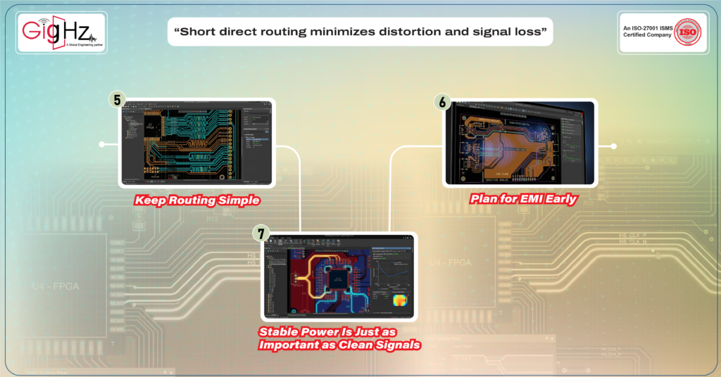
5. Keep Routing Simple
High-frequency signals prefer short, direct paths.
Complex routing increases the chance of signal distortion.
Avoid unnecessary complications such as:
- Excessive trace bends
• Long detours
• Too many vias
Each via introduces a small impedance discontinuity that can affect signal quality.
Cleaner routing practices:
- Use smooth trace transitions
• Keep critical signals short
• Match lengths in differential pairs
• Minimize layer changes
Simple routing usually leads to better electrical performance and easier debugging.
6. Stable Power Is Just as Important as Clean Signals
Signal integrity is important, but power integrity is equally critical.
In high-frequency PCB designs, circuits draw fast bursts of current when switching. If the power network cannot respond quickly, voltage noise appears. This noise can directly affect signal stability.
Key power design practices:
- Use solid power and ground planes
• Place decoupling capacitors close to power pins
• Distribute capacitors across the board
• Reduce power loop inductance
A well-designed power distribution network keeps the system electrically stable during fast switching events.
7. Plan for EMI Early
Electromagnetic interference often appears late in development, but its root cause usually starts in the layout stage.
Fast signal edges can turn traces into accidental antennas.
Ignoring EMI early may lead to compliance failures and redesigns.
Preventive layout strategies:
- Maintain continuous ground planes
• Reduce large current loops
• Route high-speed signals carefully
• Isolate noisy circuits from sensitive ones
• Add filtering where necessary
“Early EMI analysis helps identify potential issues, saving time and reducing design risks.”
Final Thoughts
High-frequency PCB design is not about adding more rules.
It is about understanding how signals behave on a real board.
A design may look perfect in the schematic.
Routing rules may pass without errors.
Early tests may even look stable.
But in real systems, signals move fast.
And the PCB layout starts influencing everything.
That is where smart design choices make a difference.
Focus on the fundamentals:
- A well-planned layer stack-up
• Clean signal paths
• Continuous return paths
• Smart component placement
• Simple routing strategies
• Stable power delivery
• Early EMI awareness
When these factors come together, the result is clear.
Cleaner signals.
Fewer debugging cycles.
More reliable hardware.
And most importantly — a PCB that works not just in the lab, but in the real world.
Need support for PCB design? Connect with our team today.
Book a Call. Schedule a Free Consultation now. https://calendly.com/gighz/30min
Stuck in a loop of challenges? Always pick smart solution that works
Have you faced costly rework because 2D drawings skipped in MCAD workflows?
Effective way to prevent MCAD documentation errors recalls?
Please answer both poll questions before submitting.
Thank you for your response! 😊
Latest Post
Get Customized Engineering CAD Design Service

Book a Free Consultation Call
Partner with Gighz and bring your most innovative design concepts to life. Our engineering cad services accelerate development so you can focus on your big vision.