

PCB Copper Thickness: What Engineers Expect vs What Actually Happens
- Posted On:
- November 3, 2026
- Category:
- Ecad

An engineer specifies 1 oz or 2 oz copper for a PCB and expects the finished board to perform accordingly.
But PCB copper thickness alone does not determine conductor performance.
The actual result depends on copper thickness, trace width, plating, etching, temperature rise, layer location, stackup, and manufacturing tolerances.
What engineers specify is not always identical to what the finished PCB delivers.
What Does PCB Copper Thickness Actually Mean?
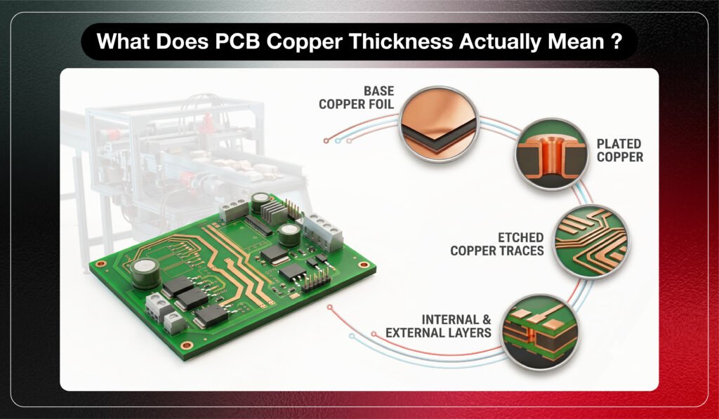
PCB copper is commonly specified as 1 oz, 2 oz, or 3 oz copper.
Copper weight refers to the mass of copper covering a defined area, while copper thickness describes its physical thickness. As a reference, 1 oz copper is approximately 35 µm thick before fabrication effects.
However, a finished trace may not have exactly that thickness.
A PCB can contain:
- Base copper foil
- Plated copper
- Etched conductors
- Internal and external copper layers
Therefore, engineers need to distinguish between nominal copper weight, base copper, and finished copper thickness.
What Engineers Expect from Copper Thickness
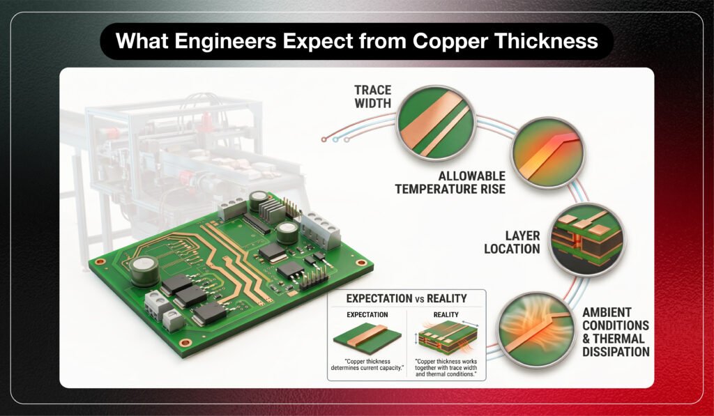
The common expectation is straightforward:
More copper = more current capacity = lower resistance.
That relationship is real, but incomplete.
Increasing copper thickness increases conductor cross-sectional area and can reduce resistance.
However, current capacity also depends on:
- Trace width
- Allowable temperature rise
- Layer location
- Ambient conditions
- Thermal dissipation
A narrow 2 oz trace does not automatically perform better than a wider 1 oz trace.
Expectation: Copper thickness determines current capacity.
Reality: Copper thickness works together with trace width and thermal conditions.
What Actually Happens During PCB Manufacturing?
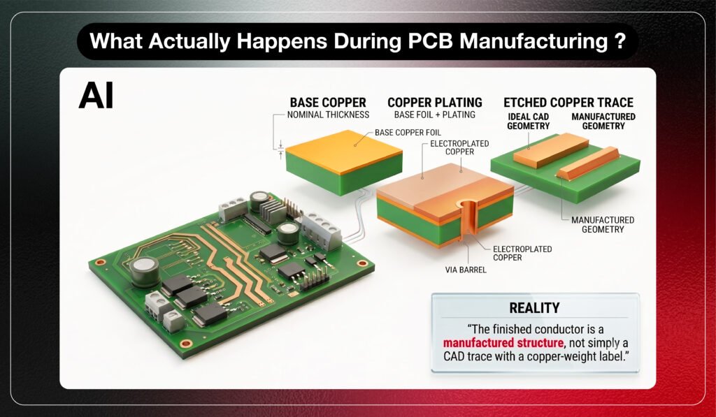
The difference becomes clearer during fabrication.
Base Copper
The board begins with copper foil having a nominal thickness. Manufacturing tolerances mean the actual starting value can vary.
Copper Plating
Outer-layer copper may receive additional plating during fabrication. Depending on the construction, the finished conductor can therefore contain base foil plus plated copper.
Etching
Etching removes unwanted copper to form the trace pattern. The resulting sidewalls may not be perfectly vertical.
Etch undercut can reduce the effective trace width compared with the ideal CAD geometry, changing the conductor’s actual cross-sectional area.
Reality: The finished conductor is a manufactured structure, not simply a CAD trace with a copper-weight label.
Does Thicker Copper Always Carry More Current?
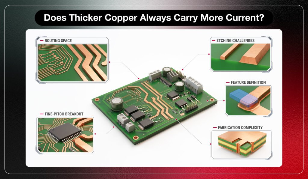
No.
Current capacity depends on how much current a conductor can carry while maintaining an acceptable temperature rise.
Cross-sectional area can be increased through greater thickness, greater width, or both.
Heavy copper can improve power handling, but it can also:
- Consume routing space
- Complicate fine-pitch breakout
- Increase etching challenges
- Affect feature definition
- Increase fabrication complexity
Design takeaway: Select copper thickness together with trace width and thermal requirements.
Copper Thickness vs Trace Width
This creates an important design trade-off.
If board space allows, increasing trace width may be more practical than immediately selecting heavy copper.
When routing space is limited, increasing copper thickness can provide additional cross-sectional area without requiring the same increase in trace width.
The correct choice depends on current, available routing area, temperature rise, layer structure, and fabrication capability.
Thickness is not a replacement for width; both are tools for controlling conductor performance.
How Copper Thickness Affects Signal Integrity
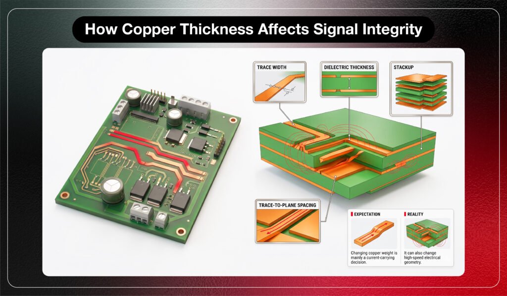
Copper thickness also affects high-speed designs.
Conductor geometry influences controlled impedance and signal loss. Changing copper thickness changes the relationship between the trace and its reference plane.
Engineers may need to adjust:
- Trace width
- Dielectric thickness
- Stackup
- Trace-to-plane spacing
A copper-weight change should therefore trigger an impedance review when controlled-impedance routing is involved.
Expectation: Changing copper weight is mainly a current-carrying decision.
Reality: It can also change high-speed electrical geometry.
Common Copper Thickness Mistakes
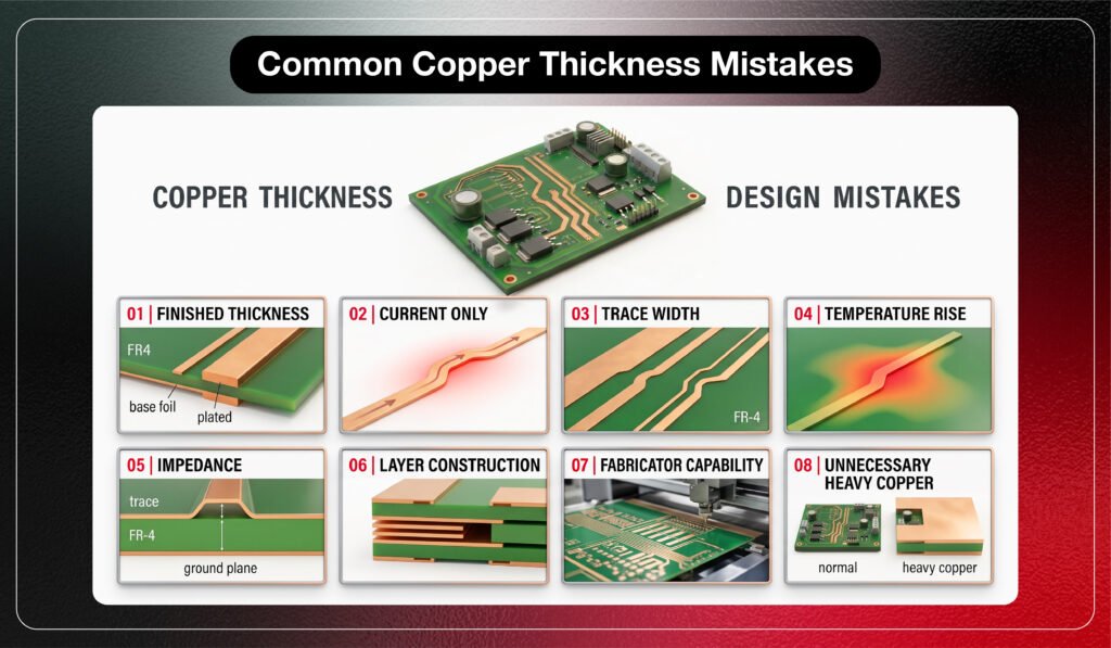
Avoid these assumptions:
- Treating copper weight as finished thickness
- Selecting thickness based only on current
- Ignoring trace width
- Forgetting temperature rise
- Changing copper weight without checking impedance
- Ignoring internal versus external layer construction
- Not confirming fabricator capabilities
- Using heavy copper where standard copper is sufficient
These mistakes can create thermal, routing, impedance, or manufacturing problems later.
When Does Heavy Copper Make Sense?
Heavy copper makes sense when substantial current or power distribution is a primary requirement.
Typical applications include:
- Power electronics
- Battery systems
- Motor-control boards
- Automotive electronics
- Industrial equipment
- High-current distribution
However, it may be unnecessary for dense digital boards dominated by fine-pitch components, narrow traces, and controlled-impedance routing.
The best copper thickness meets the electrical requirement without creating unnecessary manufacturing constraints.
Real-World Insight

Imagine selecting 2 oz copper for a high-current power path.
Later, the same board requires fine-pitch breakout and controlled-impedance routing. The heavier copper creates additional layout and manufacturing constraints that were not considered initially.
The problem is not that 2 oz copper was wrong.
The problem was treating copper thickness as an isolated specification rather than part of the complete PCB architecture.
Final Answer
Engineers often expect copper weight to directly predict finished PCB performance.
In reality, conductor behavior depends on thickness, trace width, plating, etching, temperature rise, layer construction, stackup, and fabrication capability.
PCB copper thickness should therefore be selected as part of the complete electrical and manufacturing design.
The right copper thickness is not the thickest one—it is the one that delivers the required performance within the board’s design and manufacturing constraints.
Specify copper with confidence.
Build for reliable performance.
Book a Call. Schedule a Free Consultation now. https://calendly.com/gighz/30min
Frequently Asked Questions
- What does 1 oz copper mean?
Approximately 35 µm before fabrication effects.
- Is thicker copper always better?
No. Width, thermal limits, and manufacturing also matter.
- Does copper thickness affect current capacity?
Yes, along with trace width and temperature rise.
- Does copper thickness affect impedance?
Yes. It can require trace-width or stackup adjustments.
- Why can finished copper differ?
Plating, etching, tolerances, and construction can change final geometry.
Stuck in a loop of challenges? Always pick smart solution that works
Have you faced costly rework because 2D drawings skipped in MCAD workflows?
Effective way to prevent MCAD documentation errors recalls?
Please answer both poll questions before submitting.
Thank you for your response! 😊
Latest Post
Get Customized Engineering CAD Design Service

Book a Free Consultation Call
Partner with Gighz and bring your most innovative design concepts to life. Our engineering cad services accelerate development so you can focus on your big vision.
