


A wider trace can carry more current—but width is only one part of the equation.
Every PCB trace width has resistance. As current increases, that resistance produces heat according to I²R. If the generated heat cannot dissipate effectively, the conductor temperature rises and can affect PCB reliability.
That is why current capacity depends on more than trace width. Copper thickness, temperature rise, layer position, trace length, vias, and surrounding copper all matter.
Why Does PCB Trace Width Matter?
A wider trace provides greater copper cross-sectional area, reducing resistance and helping distribute heat.
IPC-2152 provides guidance for determining conductor size based on current and acceptable temperature rise. Its approach also considers copper thickness and board construction rather than treating width as the only variable.
Here are the main factors to consider.
1. Trace Width
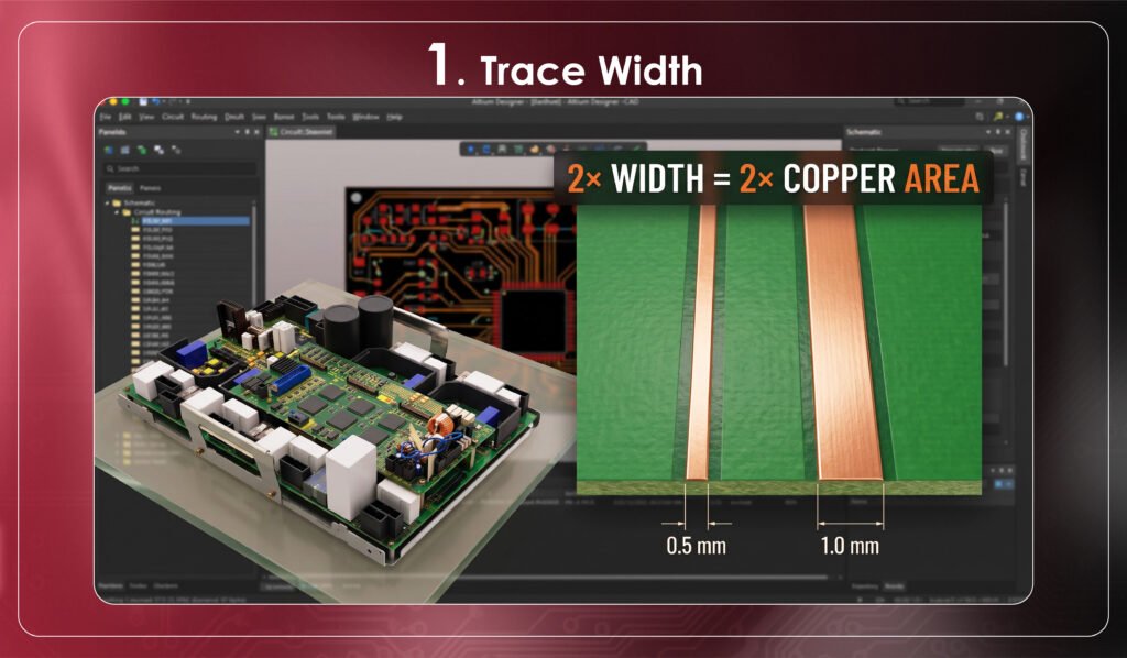
For the same copper thickness, increasing width increases cross-sectional area.
For example, increasing a 1 oz copper trace from 0.5 mm to 1 mm approximately doubles its cross-sectional area and reduces resistance per unit length.
However, current capacity does not increase in a simple 1:1 ratio with width because thermal performance depends on the complete PCB structure.
2. Copper Thickness
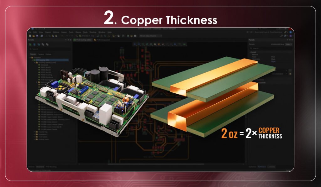
Copper thickness can provide more current capacity without consuming additional routing width.
Typical nominal values are:
- 1 oz ≈ 35 µm
- 2 oz ≈ 70 µm
Heavier copper can be useful for power paths, but fabrication capability, spacing, etching, and cost must also be considered.
3. Allowable Temperature Rise
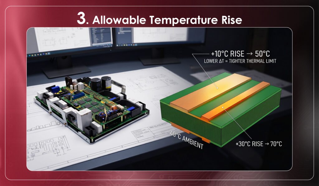
The acceptable temperature rise changes the required conductor size.
For example, with a 40°C ambient temperature, a 10°C allowable rise means targeting approximately 50°C conductor temperature. A 30°C allowance would permit approximately 70°C.
The correct limit should come from the system, component ratings, enclosure, and reliability requirements.
4. External vs. Internal Layers
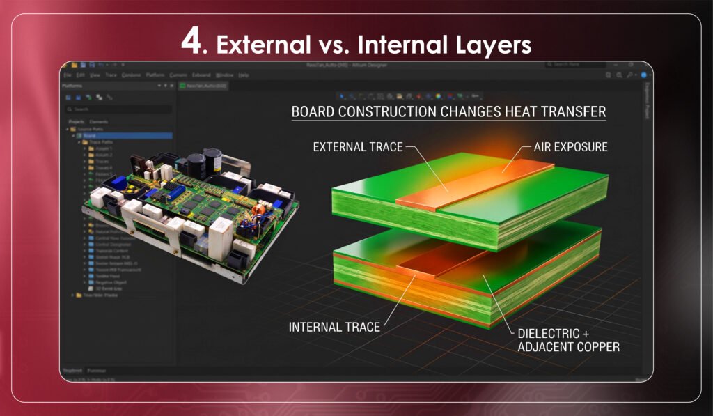
External traces generally have better access to the surrounding environment for heat transfer.
Internal traces dissipate heat differently because they are surrounded by dielectric material and adjacent copper layers.
Therefore, do not automatically apply the same assumptions to both layer types. Board construction affects thermal performance
5. Trace Length
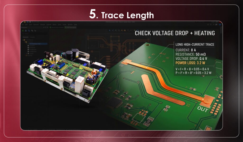
Width affects resistance per unit length, while length determines the total resistance of the path.
For example, if an 8 A path has a hypothetical resistance of 50 mΩ:
Voltage drop = 8 × 0.05 = 0.4 V
Power loss = 8² × 0.05 = 3.2 W
That 3.2 W becomes heat, so long high-current paths need both thermal and voltage-drop evaluation.
6. Vias Can Become Bottlenecks

A wide trace does not guarantee a reliable current path if it transitions through too few vias.
For high-current layer changes, multiple vias in parallel may be required. The via diameter, plating, number of vias, and surrounding copper should be considered together.
7. Avoid Narrow Neck-Downs

High-current paths often narrow around:
- Component pads
- Connector pads
- Vias
- Thermal reliefs
- Clearance areas
A 2 mm power trace that suddenly narrows to 0.3 mm can create a localized resistance and heating point.
The narrowest section of the current path deserves particular attention.
8. Use Copper Pours and Planes Where Appropriate
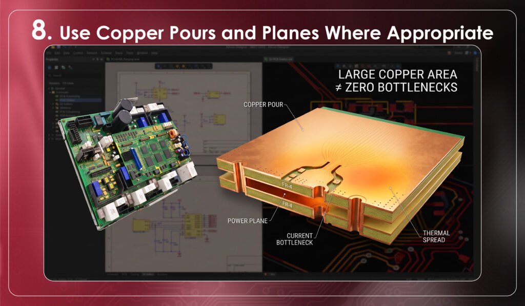
Large copper areas can help distribute current and spread heat.
Power planes and copper pours are especially useful when routing space is limited. But simply adding a large polygon does not solve every thermal problem. Connections, clearances, layer structure, and bottlenecks still need review.
9. Check Voltage Drop Separately

Thermal current capacity and voltage-drop performance are different requirements.
A trace may remain below its thermal limit while still producing too much voltage drop for a low-voltage power rail.
So, ask two questions:
- Can the conductor carry the current without excessive heating?
- Is its resistance low enough for the required voltage?
10. Validate the Complete Current Path

Before releasing a high-current design, check:
- Continuous and peak current
- Copper thickness
- Trace width and length
- Allowable temperature rise
- Internal or external layer
- Vias and transitions
- Component and connector pads
- Copper planes and pours
- Ambient temperature
- Voltage drops
For demanding applications, thermal analysis or measurement on a representative board can provide additional validation.
PCB Trace Width Design Checklist
Before fabrication, verify that:
- Current requirements are defined
- Temperature-rise limits are established
- Copper thickness matches fabrication capability
- Trace width is suitable for the actual stackup
- Long paths are checked for voltage drop
- Vias can handle the required current
- Narrow neck-downs are identified
- Power planes or pours are used were beneficial
- Connectors and component transitions are reviewed
- Thermal performance is validated
Conclusion
PCB trace width affects current capacity because it changes copper area, resistance, and heat generation.
But width alone does not determine whether a current path is reliable.
Copper thickness, temperature rise, layer position, length, vias, planes, and voltage drop all influence the final design.
For high-current boards, treat trace sizing as a complete power-path and thermal-design problem, not simply a width calculation.
Reliable Current. Better PCB Performance.
Validate Your Trace Width Today.
https://gighz.net/contact-us/
Book a Call. Schedule a Free Consultation now. https://calendly.com/gighz/30min
Frequently Asked Questions
- Does a wider trace always carry more current?
Generally, yes when other conditions remain similar. More copper area reduces resistance and heating.
- Is copper thickness important?
Yes. Increasing copper thickness increases cross-sectional area without requiring additional routing width.
- Are internal and external traces equivalent?
No. Their thermal environments differ, so the actual board construction must be considered.
- Can a wide trace still overheat?
Yes. Vias, pads, connectors, or narrow neck-downs can become bottlenecks.
Stuck in a loop of challenges? Always pick smart solution that works
Have you faced costly rework because 2D drawings skipped in MCAD workflows?
Effective way to prevent MCAD documentation errors recalls?
Please answer both poll questions before submitting.
Thank you for your response! 😊
Latest Post
Get Customized Engineering CAD Design Service

Book a Free Consultation Call
Partner with Gighz and bring your most innovative design concepts to life. Our engineering cad services accelerate development so you can focus on your big vision.
