


Nearly 60–70% of PCB fabrication re-spins happen due to rule violations that were not caught during design stage validation, even when the layout appears correct and passes basic inspection.
A PCB can look correctly routed in the layout editor, pass visual checks, and even pass electrical simulation, yet still fail during fabrication or field testing.
This happens because visual correctness is not equal to manufacturing correctness.
That gap is exactly where PCB Design Rule Check (DRC) becomes critical — it ensures the design is manufacturable, electrically stable, and production-ready before fabrication begins.
What Is Design Rule Checking?
Design Rule Checking is an automated process that validates a PCB layout against manufacturing, electrical, and assembly rules.
These rules are typically set based on real fabrication capabilities such as:
- Minimum trace width
- Minimum clearance
- Via drill size limits
- Annular ring
- Copper-to-edge spacing rules
- High-voltage isolation spacing
Modern PCB tools continuously check these rules during routing to ensure manufacturability.
How Design Rule Checking Works
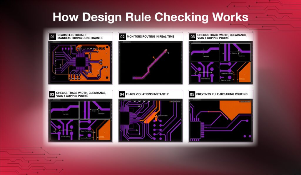
PCB design tools such as Altium Designer, KiCad, OrCAD, Cadence Allegro, Autodesk EAGLE, Siemens Xpedition, and other professional EDA tools use rule-based engines to analyze PCB layouts.
The process includes:
- Reads electrical and manufacturing constraints
- Monitors routing in real time
- Checks trace width, clearance, vias, and copper pours
- Flags violations instantly in the layout view
- Prevents rule-breaking routing before completion
Each violation is marked directly on the layout, allowing designers to fix issues immediately rather than discovering them during manufacturing.
Why DRC Matters for PCBs
A PCB may look correct in the layout but still contain hidden issues like trace width errors, spacing violations, via size mistakes, or poor component placement.
These issues are difficult to detect manually, especially in complex or high-speed designs.
DRC automatically checks the entire layout against design rules to ensure it is manufacturable and compliant.
It helps prevent fabrication failures, prototype issues, redesign costs, and improves first-pass success and overall reliability.
What Problems Does DRC Prevent in PCB Design?
1. Manufacturing Rule Violations
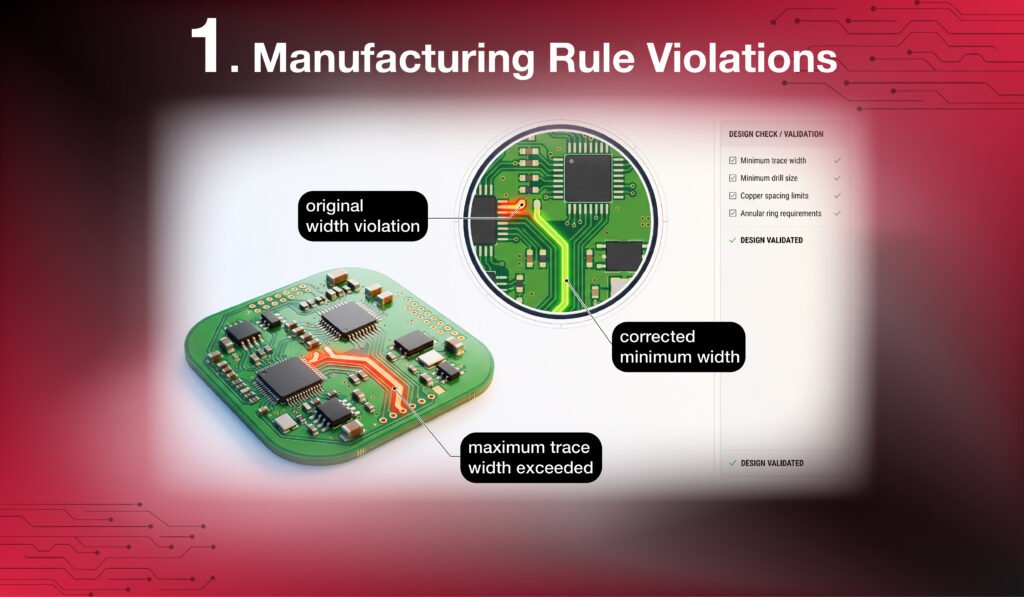
PCB manufacturers follow strict fabrication constraints such as:
- Minimum trace width
- Minimum drill size
- Copper spacing limits
- Annular ring requirements
If these rules are violated, the design may be rejected or require modification before production.
DRC ensures compliance before sending files to manufacturing.
2. Electrical Short Circuits

Two nets may appear safely separated visually but still violate minimum clearance rules.
This can lead to:
- Short circuits during fabrication
- Signal interference
- Board failure during testing
These violations are detected early in the workflow.
3. Signal Integrity Risks
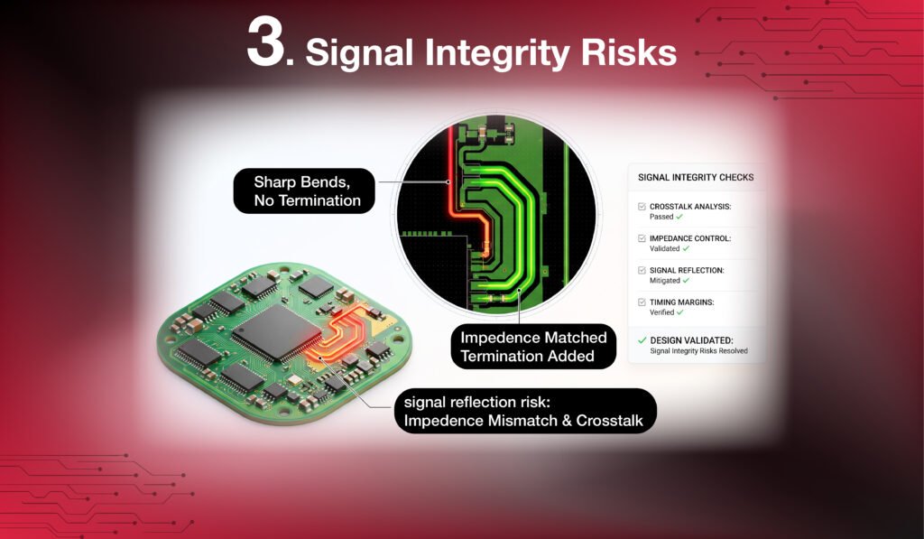
In high-speed designs, layout geometry directly impacts electrical behavior.
Improper spacing or routing can lead to:
- Crosstalk between traces
- Impedance discontinuities
- Signal reflections
- Timing errors
DRC enforces spacing rules that help reduce these risks early.
4. Assembly and Placement Issues
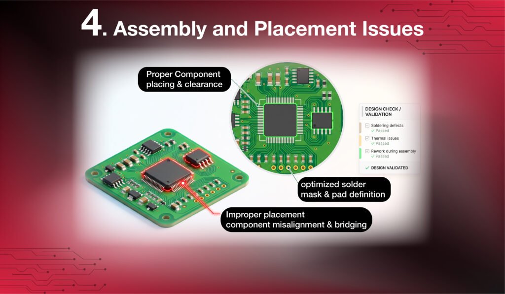
Component spacing is critical for automated assembly and soldering.
Improper placement can cause:
- Soldering defects
- Thermal issues
- Rework during assembly
DRC ensures components follow assembly-friendly spacing rules.
5. Power and Thermal Constraints

High-current traces require sufficient copper width and proper routing paths.
If not designed correctly, this can result in:
- Overheating
- Voltage drops
- Reliability degradation
DRC ensures power routing follows defined electrical limits.
Why Manual Checking Is Not Enough
Manual PCB review is still useful, but it has clear limitations.
Modern PCB designs include:
- Thousands of nets
- Multiple layers
- High-density routing
- Fine-pitch components
- High-speed interfaces
In such complexity, manual inspection becomes:
- Time-consuming
- Inconsistent
- Error-prone
Even experienced engineers can miss small violations that lead to critical failures.
DRC eliminates this uncertainty by applying consistent, rule-based validation across the entire design
Common Mistake in PCB Design Workflow
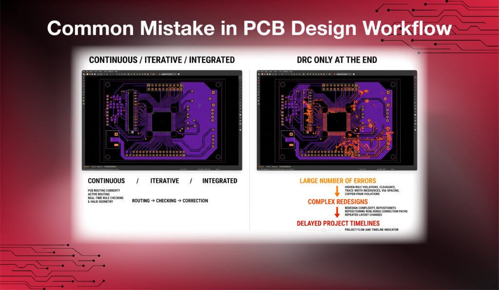
One of the most common mistakes engineers make is treating DRC as a final step before fabrication.
In reality, it should be:
- Continuous
- Iterative
- Integrated into the design process
Running it only at the end often leads to:
- Large numbers of errors
- Complex redesigns
- Delayed project timelines
Using it throughout routing ensures issues are detected early when they are easier to fix.
How Design Rule Checking Improves Reliability

Reliable PCB performance depends on consistency across electrical, mechanical, and manufacturing conditions.
DRC contributes directly by improving:
- First-Pass Success Rate
Early detection of violations reduces prototype failures and redesign cycles.
- Manufacturing Yield
Designs that follow fabrication constraints produce fewer defects during production.
- Electrical Stability
Proper spacing and routing improve signal integrity and reduce noise.
- Cost Efficiency
Early error detection reduces fabrication waste and redesign costs.
Real-World Insights
Most PCB failures are not caused by component issues but by layout-level violations.
A design can:
- Pass simulation
- Pass schematic validation
- Appear correct visually
Yet still fail in manufacturing due to hidden rule violations.
This is why DRC is not optional in modern PCB workflows—it is a core reliability mechanism.
Final Answers
PCB Design Rule Check ensures that a PCB layout is not only logically correct but also manufacturable, electrically stable, and assembly-ready.
Without it, even well-designed boards can fail due to:
- Clearance violations
- Manufacturing rule mismatches
- Signal integrity issues
- Power routing problems
By integrating it throughout the design process, engineers can significantly improve first-pass success, reduce failures, and ensure long-term reliability.
In modern PCB design, reliability does not come from assumption.
Contact us to ensure error-free, reliable PCB designs with proper DRC validation.
https://gighz.net/contact-us/
Book a call. Schedule a Free Consultation now. https://calendly.com/gighz/30min
FAQ
1. What is PCB Design Rule Check?
It is an automated check that ensures PCB layouts follow manufacturing and electrical design rules.
2. Why is DRC important?
It helps detect design errors early and improves manufacturing success and reliability.
3. What issues does DRC detect?
It detects clearance violations, trace width issues, short circuits, and via errors.
4. Can a PCB pass DRC but still fail?
Yes. Signal integrity or stackup issues can still cause failures even after DRC passes.
5. Is DRC enough for reliable PCB design?
No. It must be combined with signal integrity and proper stackup planning for full reliability.
Stuck in a loop of challenges? Always pick smart solution that works
Have you faced costly rework because 2D drawings skipped in MCAD workflows?
Effective way to prevent MCAD documentation errors recalls?
Please answer both poll questions before submitting.
Thank you for your response! 😊
Latest Post
Get Customized Engineering CAD Design Service

Book a Free Consultation Call
Partner with Gighz and bring your most innovative design concepts to life. Our engineering cad services accelerate development so you can focus on your big vision.
