

The Truth About High-Speed PCB Design That Saves Weeks of Debugging
- Posted On:
- October 26, 2026
- Category:
- Ecad

Every PCB project starts with confidence. The schematic is complete, the layout looks good, and the board is ready for manufacturing.
Then the prototype arrives.
USB drops data. DDR memory fails to initialize. Ethernet becomes unstable. EMI testing fails.
In high-speed PCB design, even small layout mistakes can create big performance problems. The good news is that most of these issues can be avoided before manufacturing.
Before the First Prototype
Many high-speed PCB problems begin long before testing starts. Before sending your PCB for manufacturing, check for these common issues:
- No signal integrity analysis
- Controlled impedance not defined
- Poor differential pair routing
- Return paths crossing split planes
- Components placed without routing constraints
- DFM checks not completed
Ignoring these issues can lead to failed testing, PCB re-spins, and weeks of debugging.
The Truth #1: DRC Isn't Enough
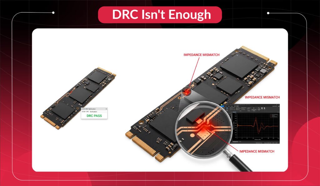
Many designers believe a clean Design Rule Check means the board is ready for production. While DRC is essential, it only verifies physical constraints. It does not validate electrical performance.
A board can still contain a critical design error even after passing every DRC.
DRC cannot detect:
- Signal timing violations
- Return path discontinuities
- Crosstalk between critical signals
- Impedance mismatch
- Power integrity problems
These issues often remain hidden until prototype fabrication, when fixing them usually requires another board spin and an expensive redesign cycle.
The Truth #2: Plan Signal Integrity Early
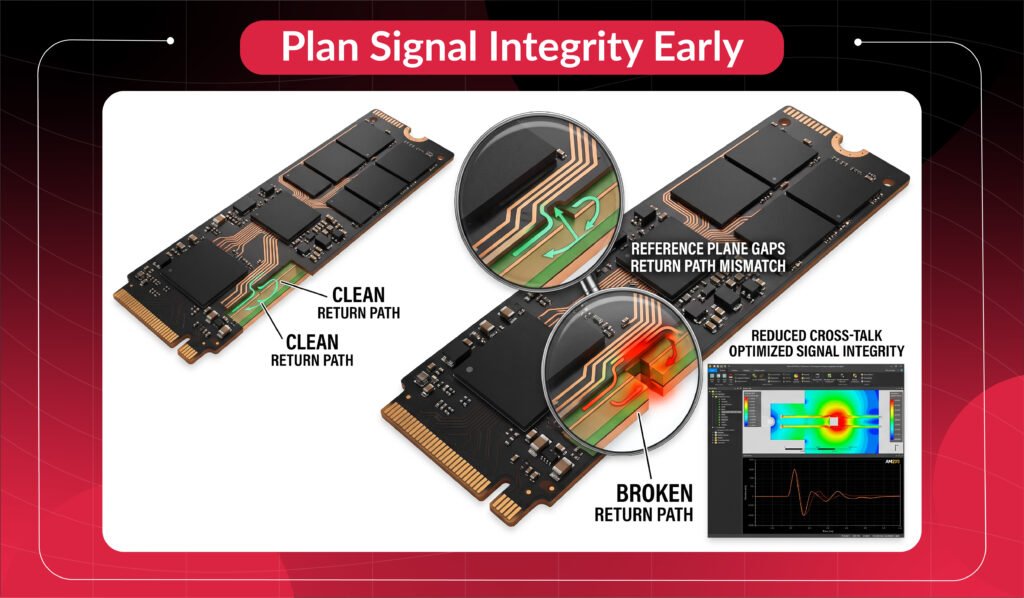
One of the biggest misconceptions in modern PCB layout is that signal integrity becomes important only after routing begins. In reality, it starts during the planning stage.
A successful high-speed layout depends on:
- Selecting the correct PCB stackup
- Defining controlled impedance early
- Maintaining continuous reference planes
- Planning clean return current paths
- Reducing unnecessary layer transitions
Without this foundation, even perfectly routed traces can suffer from reflections, ringing, and unstable communication.
The Truth #3: Placement Comes First
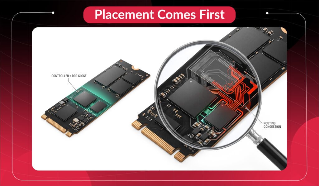
Routing rarely fixes poor component placement. Most routing challenges are created before the first trace is drawn.
Good placement should focus on:
- Keeping processors and DDR memory close together
- Positioning high-speed connectors for shorter routing paths
- Placing decoupling capacitors close to power pins
- Ensuring proper mechanical fit
- Verifying component libraries before layout
A small footprint mistake or poor placement decision can delay manufacturing and create difficult-to-diagnose hardware issues.
The Truth #4: Every Routing Decision Matters
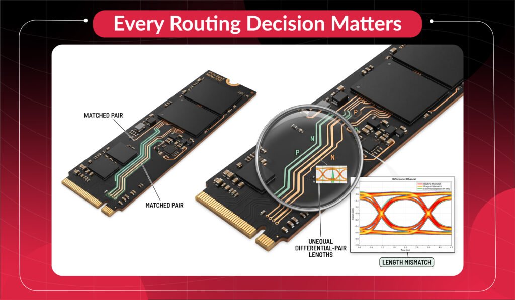
Reliable high-speed boards are built through hundreds of careful routing decisions.
Common mistakes include:
- Unequal differential pair lengths
- Inconsistent trace widths
- Excessive vias on critical signals
- Broken return paths
- Poor solder mask clearance
- Routing across split ground planes
Each mistake may appear minor, but together they can reduce signal quality, increase EMI, and lead to unstable system performance.
The Truth #5: Simulate Before You Build
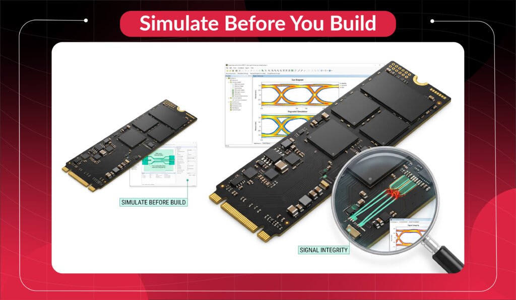
Many teams skip simulation because they think it slows development. In reality, simulation shortens project schedules by identifying problems before hardware is built.
Simulation helps engineers verify:
- Signal integrity
- Power integrity
- Timing margins
- Reflection and crosstalk
- Controlled impedance performance
Finding these issues during design is far less expensive than discovering them after manufacturing.
Best Practices That Prevent Weeks of Debugging
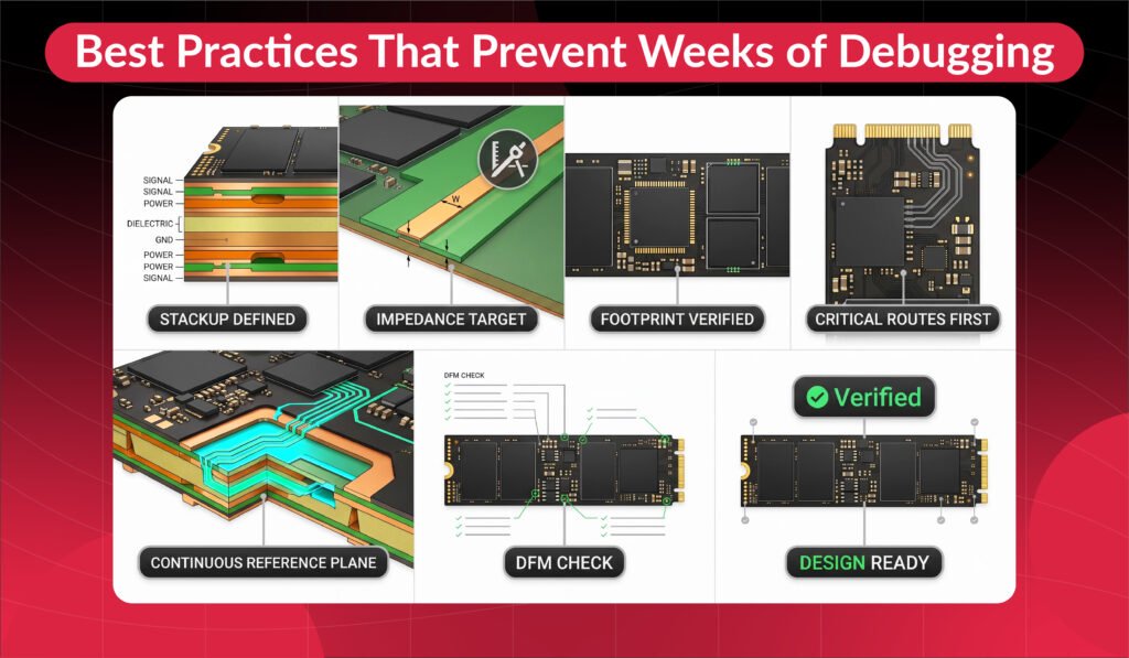
Successful PCB design projects begin with planning instead of repair.
Before releasing your design:
- Define the PCB stackup before routing.
- Establish impedance targets early.
- Verify footprints and component libraries.
- Route critical interfaces before general signals.
- Maintain continuous reference planes.
- Complete DFM checks before manufacturing.
- Review the design for electrical and manufacturing readiness.
Every one of these steps reduces project risk and improves first-pass success.
Final Thought
The biggest misconception about High-Speed PCB design is that success depends on routing faster.
In reality, successful designs come from making better engineering decisions earlier in the process.
Careful stackup planning, proper component placement, continuous return paths, simulation, and thorough verification all contribute to a reliable board.
Every hour spent improving the layout can save days of debugging after fabrication.
By following proven PCB design practices, engineering teams can reduce costly redesigns, accelerate development, and deliver products that work right the first time.
Reduce debugging and accelerate development.
Get in touch for reliable PCB design support.
Want to avoid hidden issues in your design?
Connect with us for the expert free consultation
https://calendly.com/gighz/30min
Stuck in a loop of challenges? Always pick smart solution that works
Have you faced costly rework because 2D drawings skipped in MCAD workflows?
Effective way to prevent MCAD documentation errors recalls?
Please answer both poll questions before submitting.
Thank you for your response! 😊
Latest Post
Get Customized Engineering CAD Design Service

Book a Free Consultation Call
Partner with Gighz and bring your most innovative design concepts to life. Our engineering cad services accelerate development so you can focus on your big vision.
