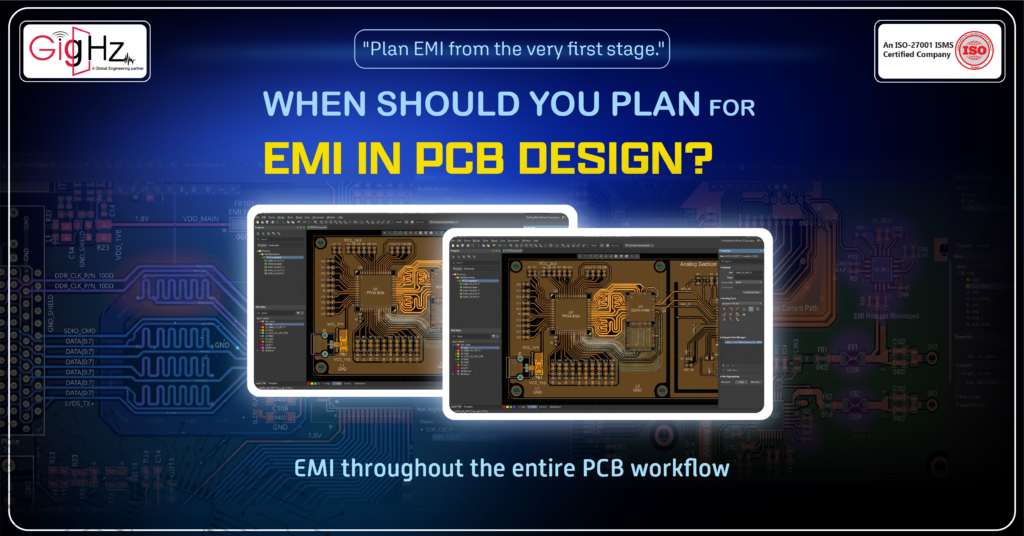
When Should You Plan for EMI in PCB Design?
- Posted On:
- June 25, 2026
- Category:
- Analysis & Simulation
Electromagnetic interference (EMI) is one of the biggest hidden challenges in electronics design.
Many engineers think EMI only matters during the final stages or after manufacturing. In practice, EMI should be addressed at the very start of PCB design, not just at the end.
Most EMI problems start during early design stages, and planning for EMI can prevent noise issues once the board is powered.
That’s why experienced engineers plan for EMI throughout the entire PCB workflow, not just at the end.
Modern high-speed systems, compact designs, and switching power circuits all increase EMI risk. Even a single long trace or missing decoupling capacitor can create problems later.
When should you actually plan for EMI in PCB design?
The short answer? From the very beginning.
Let’s break down what that really means.
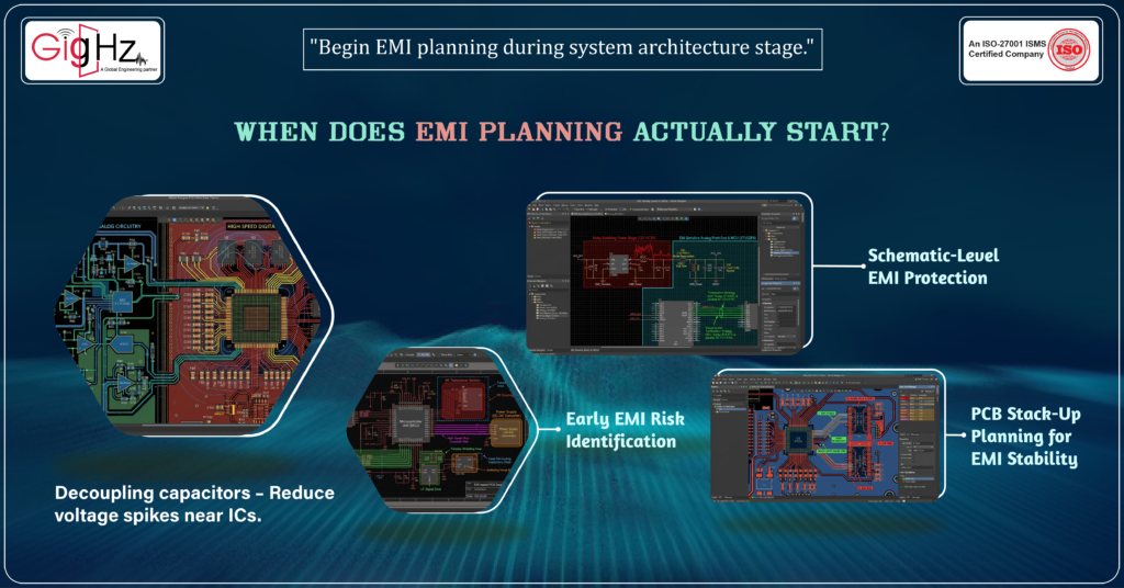
When Does EMI Planning Actually Start?
EMI planning should begin as early as the system architecture stage and continue through every step of PCB design.
Key stages and when to act for EMI in PCB Design:
System architecture – Decide blocks, interfaces, and power systems. This is when you spot potential EMI sources.
Schematic design – Add EMI protection components like decoupling capacitors and filters. This is the stage for basic noise suppression.
PCB stack-up planning – Arrange signal, power, and ground layers to minimize radiation. Now you define return paths and layer separation.
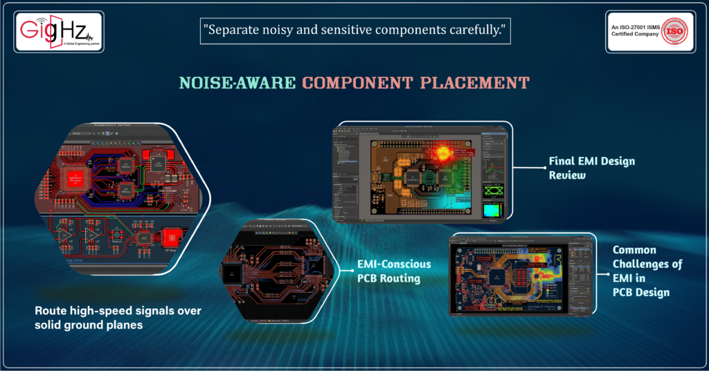
Component placement – Separate noisy circuits from sensitive ones. This is when placement decisions affect EMI most.
PCB routing – Optimize return paths, trace length, and impedance. Routing decisions directly control EMI loops.
Final design review – Verify EMI measures were applied correctly. This is the last check before manufacturing.
Ignoring EMI until the final stages can lead to redesigns, extra shielding, or compliance failures, which are costly and time-consuming.
Acting at the right time during each stage ensures informed design choices and fewer surprises later.
Early EMI Risk Identification
When: System architecture stage
Goal: identify potential EMI sources before layout begins.
Common EMI risk factors:
- High-speed digital interfaces – Fast edges generate high-frequency noise.
- Switching power supplies – Produce broad-spectrum EMI if unfiltered.
- High-frequency clock signals – Can couple into analog or RF circuits.
- Wireless modules – Transmit/receive RF signals, susceptible to interference.
- Long cable connections – Act as antennas, increasing radiated noise.
Why it matters:
- Allows engineers to plan grounding and shielding
- Helps separate noisy and sensitive circuits at the system level.
- Prevents costly rework downstream.
Even choosing lower-frequency components or isolating analog sections can significantly reduce EMI risks at this stage.
Schematic-Level EMI Protection
When: During schematic design
Purpose: control noise at the source and stabilize signals.
Common EMI components:
- Decoupling capacitors – Reduce voltage spikes near ICs.
- Bulk capacitors – Handle large current changes.
- Ferrite beads – Block high-frequency noise on power and signal lines.
- EMI filters / chokes – Suppress unwanted noise and prevent it from spreading.
Why it matters:
- Proper capacitor placement dramatically reduces radiated noise.
- Termination resistors on high-speed lines minimize reflections, which otherwise increase EMI.
- Adding these components in the schematic ensures layout engineers can manage EMI later.
Even small adjustments, like placing a capacitor near a high-speed IC or adding a ferrite bead on a power line.
PCB Stack-Up Planning for EMI Stability
When: During stack-up planning
Stack-up defines how signal, power, and ground layers are arranged.
A well-designed stack-up ensures:
- Stable signal return paths
- Reduced electromagnetic radiation
- Improved signal integrity
- Better thermal performance
Best practices:
- Solid ground planes – provide stable reference for signals.
- Signal layers close to ground – minimize loop areas.
- Avoid split planes – splits create unwanted current loops.
- Short return paths – reduce radiated EMI.
Why it matters:
- Smaller loop areas = less EMI
- Proper stack-up reduces signal coupling, especially in multilayer boards
- Maintains consistent impedance for high-speed traces
Finalizing stack-up before routing avoids having to move traces or split planes later.
Noise-Aware Component Placement
When: During placement
Goal: separate noisy components from sensitive ones.
Noisy components:
- Switching regulators
- High-speed processors
- Clock generators
Sensitive components:
- Analog amplifiers
- Sensors
- RF modules
Placement rules:
- Keep noisy components away from analog circuits
- Place oscillators near their ICs
- Separate analog and digital areas
- Put decoupling capacitors close to IC power pins
Why it matters:
- Reduces interference paths
- Simplifies routing, especially high-speed or differential pairs
- Small adjustments, like rotating components, can significantly reduce coupling
Even a few millimetres of separation can improve EMI performance.
EMI-Conscious PCB Routing
When: During routing
Every signal trace forms a current loop with its return path.
Large loops = more EMI.
Routing tips:
- Route high-speed signals over solid ground planes
- Avoid crossing split planes
- Keep traces short whenever possible
- Maintain controlled impedance
Extra considerations:
- Space noisy and sensitive traces apart
- Use multiple layers for ground and power
- Route return paths directly under the signal trace
- Minimize vias on high-speed lines
Why it matters:
- Predictable return paths reduce radiated noise
- Careful routing ensures signals behave as intended, even on high-speed boards
Final EMI Design Review
When: Just before manufacturing
Check all EMI measures:
- Ground plane continuity
- Decoupling capacitor placement
- High-speed signal routing
- Power distribution layout
Optional but recommended:
- Signal integrity simulations
- Power integrity analysis
- Pre-compliance EMC simulations
Why it matters:
- Early detection prevents costly redesigns
- Ensures your design is ready for manufacturing and regulatory requirements while maintaining strong compliance.
Common Challenges of EMI in PCB Design
Even careful designs can face issues:
- Poor grounding
- Long signal return paths
- Missing decoupling capacitors
- Crosstalk between traces
- Long high-speed signal runs
Addressing these issues early in design helps maintain signal integrity and ensures the board functions reliably.
Final Thoughts
EMI should never be a last-minute concern.
It needs attention from the very beginning — during system architecture, schematic, stack-up, component placement, routing, and final review.
Planning for EMI early reduces redesigns and ensures your board works reliably under all conditions.
Boards designed with EMI in mind are more stable, easier to manufacture, and more likely to meet EMC requirements the first time.
By considering EMI in PCB Design at every stage, engineers can build robust, high-quality PCB designs that perform consistently in real-world environments.
Early EMI planning is the key to stable, high-performance, and reliable PCB designs.
Planning a PCB project? Let’s help you design it right from the start.
Get in touch with our team to discuss your design needs- https://gighz.net/contact-us/
Book a Call. Schedule a Free Consultation now. https://calendly.com/gighz/30min
Stuck in a loop of challenges? Always pick smart solution that works
Have you faced costly rework because 2D drawings skipped in MCAD workflows?
Effective way to prevent MCAD documentation errors recalls?
Please answer both poll questions before submitting.
Thank you for your response! 😊
Latest Post
Get Customized Engineering CAD Design Service

Book a Free Consultation Call
Partner with Gighz and bring your most innovative design concepts to life. Our engineering cad services accelerate development so you can focus on your big vision.