Top 10 Printed Circuit Board Design Rules for Student Hardware Teams
- Posted On:
- February 25, 2026
- Category:
- Ecad
When student hardware teams build their first real printed circuit board design rules, the excitement is high—but so is the chance of making mistakes that silently break the design.
A tiny gap in the ground plane, one long high-speed trace, or a misplaced decoupling capacitor can turn a promising project into hours of debugging.
Many teams learn these lessons only after a board fails during testing, or worse, just before a competition.
PCB design is not about making the board look stylish.
It is about doing things correctly so the board works without noise or errors.
These 10 rules are the core principles every student team should follow.
They protect your design from noise, heat, timing issues, and manufacturing errors.
And most importantly—they help you deliver a board that works the first time.
1. Maintain a Continuous, Unbroken Ground Plane
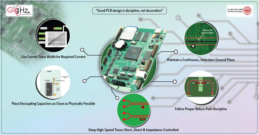
A stable ground plane is the foundation of clean signal flow.
When the ground plane is cut by routing or shapes, it forces the return current to take a longer, unpredictable path.
This increases loop area, EMI, ringing, and can even create ground bounce in sensitive circuits.
Keep one full, continuous ground plane whenever possible. Avoid splitting it unless you have a specific mixed-signal reason.
Even then, think carefully before dividing. A quiet, uninterrupted ground plane gives your design a strong base that supports all other rules.
2. Follow Proper Return Path Discipline
Many students assume current returns through the “shortest path,” but in reality, it follows the path of least impedance.
This means return current travels directly under the signal trace when a good reference plane exists.
If a trace jumps to another layer without a nearby via to connect the return path, the current is forced around gaps or plane splits. This increases noise and reduces signal integrity.
So, always keep a continuous reference plane below high-speed traces and add stitching vias to support clean return paths.
A signal is never alone—its return path must travel with it.
3. Keep High-Speed Traces Short, Direct & Impedance-Controlled
High-speed interfaces like USB, HDMI, Ethernet, DDR, and LVDS do not forgive poor layout.
These signals behave more like controlled energy waves than simple voltages.
Follow these rules strictly:
- Maintain differential impedance
- Match lengths where required
- Avoid stubs
- Keep traces short and direct
- Stay on a consistent reference plane
- Use minimal vias
Ignoring these rules can cause data errors, timing failures, and unpredictable behavior.
High-speed design is not about looks; it is about discipline and careful geometry.
4. Place Decoupling Capacitors as Close as Physically Possible
A decoupling capacitor becomes weaker every millimeter it moves away from the IC pin.
Its job is to supply instant current during switching events, but long connections add unwanted inductance.
The rule is simple:
IC power pin → shortest path → Capacitor → ground via.
Do not use long traces or place capacitors far from the pin just for neatness. Good decoupling is quiet and practical. Place it tight and direct.
5. Use Correct Trace Width for Required Current
Current density is often overlooked in student projects. A trace that looks strong on screen may not survive real loads.
Undersized traces heat up, drop voltage, or in the worst case burn during high current conditions.
Use IPC-2221 or IPC-2152 trace-width charts to calculate proper width.
Consider:
- current load
- copper thickness
- allowed temperature rise
A safe trace is not an artistic choice—it is a calculated decision.
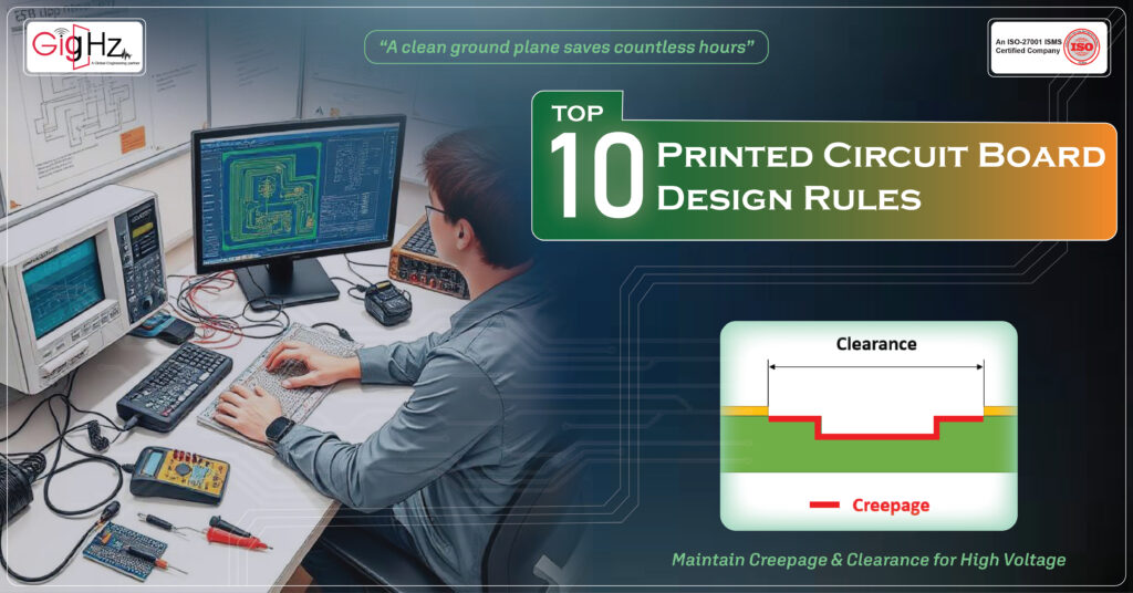
6. Maintain Creepage & Clearance for High Voltage
High-voltage circuits need physical spacing to avoid arcing or shorting, especially in humid or dusty environments.
Creepage (surface distance) and clearance (air distance) protect both the user and the circuit.
Follow IEC/UL standards for:
- minimum spacing
- isolation slots
- PCB barriers
Student teams often reduce spacing to fit everything on a small PCB, but safety must come first. Good spacing is non-negotiable.
7. Avoid 90° Trace Angles
Ninety-degree corners look harmless, but they introduce multiple issues:
- impedance discontinuity for high-speed signals
- EMI hotspots
- potential acid traps in manufacturing
Use 45° angles or smooth curves. They give cleaner routing and support more stable signal flow.
This small change keeps your board healthier during both operation and fabrication.
8. Keep Analog, Digital & Power Sections Separated
Mixed-signal PCBs often fail because noisy digital circuits pollute sensitive analog areas.
Switching regulators, motors, and high-frequency clocks can easily corrupt sensor readings.
Divide your PCB into clear zones:
- Analog
- Digital
- Power
Route their grounds so they return to a common point without crossing into each other’s regions.
Good zoning gives every signal group its own safe space to breathe.
9. Use a Proper Via Strategy
Vias are not just holes; they are electrical and thermal elements that affect performance.
Follow smart via practices:
- Use via-in-pad only if your manufacturer supports filled and plated vias
- Do not route high-speed signals across plane splits
- Use backdrilling for extremely high-speed traces if available
- Add thermal vias under power devices for heat removal
Random or careless via placement leads to thermal imbalance, poor return paths, and higher EMI.
10. Perform DRC & DFM Checks Before Fabrication
Skipping checks is one of the most common student mistakes.
DRC (Design Rule Check) catches electrical and layout errors.
DFM (Design for Manufacturing) confirms that your PCB vendor can actually build the board.
Check for:
- minimum trace/space
- annular ring sizes
- drill-to-copper limits
- solder mask openings
- via-to-pad spacing
A clean DRC/DFM report saves money, avoids re-ordering, and gives your team confidence before sending files to fabrication.
Bottom Line
Great PCBs don’t appear through doing PCB design with correct rules —they come from discipline and thoughtful engineering.
These 10 rules help student hardware teams avoid common problems and build designs that work reliably in real tests, competitions, and research projects.
When you apply these principles with care, your printed circuit board design rules becomes more stable, more predictable, and far easier to debug.
Every board you build is a step toward becoming a better designer. Start with these fundamentals and you’ll build hardware your whole team can trust.
Book a Call. Schedule a Free Consultation now. https://calendly.com/gighz/30min
Stuck in a loop of challenges? Always pick smart solution that works
Have you faced costly rework because 2D drawings skipped in MCAD workflows?
Effective way to prevent MCAD documentation errors recalls?
Please answer both poll questions before submitting.
Thank you for your response! 😊
Latest Post
Get Customized Engineering CAD Design Service

Book a Free Consultation Call
Partner with Gighz and bring your most innovative design concepts to life. Our engineering cad services accelerate development so you can focus on your big vision.