What Goes On Behind Your PCB Project When It’s Handled by a White Labelling Partner
- Posted On:
- February 20, 2026
- Category:
- Ecad

Most agencies, industrial design studios, IoT solution providers, and electronics service companies want to offer PCB design to their clients — but not everyone has an in-house engineering team.
This is where white labeling becomes powerful.
When you outsource your PCB projects to a backend engineering team like ours, your client sees your brand, your expertise, and your delivery quality — while we do the heavy technical lifting silently behind the scenes.
But what actually happens behind your PCB project once you hand it over to a white-label engineering partner?
This blog breaks down the complete behind-the-scenes process so you know exactly what happens, how your brand remains protected, and how the work stays consistent, fast, and fully compliant with your client expectations.
1. Translating Your Client Brief Into Engineering Inputs

Most agencies hand over a client requirement that is either incomplete, unclear, or missing PCB-level details.
Our first step is always, where we convert your client’s high-level idea into clear technical inputs.
What happens behind the scenes:
- We extract missing electrical parameters
- Identify risk areas, signal-speed constraints, and routing bottlenecks
- Check feasibility and manufacturability
- Request any missing documents silently (you forward them to us — the end client never knows)
What this means for you (white-label partner):
✔ You look technically strong in front of your client
✔ No risk of embarrassing back-and-forth
✔ You save hours of clarification work
2. BOM Review & Component Engineering
Even if your client sends a BOM, it’s usually incomplete or non-DFM.
We perform:
- Lifecycle check (EOL/NRND alerts)
- Availability check
- Parametric validation
- Package verification
- Alternate component suggestions
All of this is delivered under your brand.
You Get:
- A BOM your client thinks you optimized
- Zero supply-chain surprises during prototype
- Faster movement into schematic capture
3. Schematic Capture Under Your Brand Guidelines
We match your template, symbol standards, naming conventions, and company formatting rules.
Behind the scenes, we handle:
- Hierarchical design
- Power tree planning
- High-speed constraints
- Reference design checks
- EMC-aware schematic decisions
You Get:
✔ A clean schematic with YOUR logo
✔ Ready to send to your client
✔ Zero engineering manpower required from your side
4. Pre-Layout Constraint Planning (Where Most Agencies Struggle)
Before routing begins, we create a constraint document to avoid redesign delays.
We prepare:
- Stackup recommendations
- Impedance profiles
- Routing widths / clearances
- SI/PI-sensitive regions
- Thermal-sensitive zones
- EMI guard rules
You Look Like This to Your Client:
“A well-prepared engineering company with a strong pre-layout approach.”
5. PCB Layout Execution — The Real White-Label
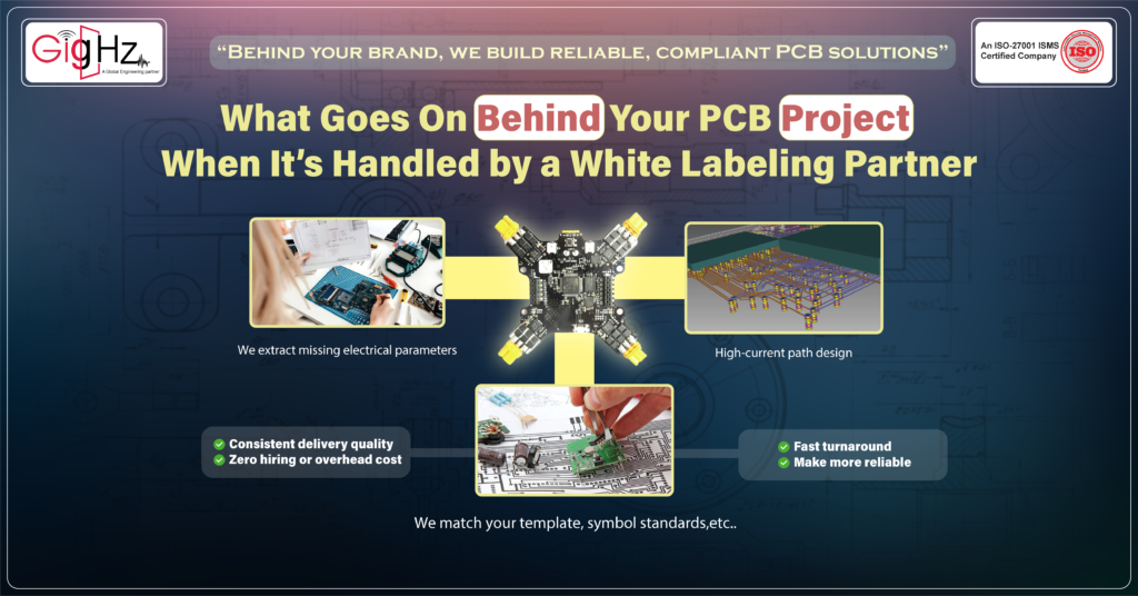
This is where your “invisible team” works at full speed.
What we handle quietly:
- Placement optimization
- Routing
- High-current path design
- DDR/SerDes/USB/HDMI routing
- RF-sensitive routing
- Power integrity improvements
- Grounding & noise control
- Thermal relief planning
- DFM + DFT compliance checks
This is the stage where we spend the most hours so you don’t have to hire a PCB layout engineer.
For You:
✔ Fast delivery
✔ Zero internal engineering load
✔ Happy end clients
6. Simulation & Verification

Most white-label partners cannot offer simulation.
You can — because we run them under your name.
We quietly run:
- Signal Integrity analysis
- Power Integrity analysis
- Thermal simulations
- EMI pre-compliance checks
Your Client Thinks:
“You do advanced verification.”
(Because everything is delivered using your branding.)
7. Fab Package Preparation
We generate a client-ready manufacturing package with YOUR logo:
- Gerbers
- Drill files
- Fab drawing
- Assembly drawing
- Pick & place
- 3D step
- BOM
- Stackup
- Impedance certificate (if needed)
You Get:
✔ A professional Fab package
✔ Ready to send directly to your client
✔ Zero engineering hours spent by you
8. Behind-the-Scenes Communication & NDA Protection
Your client never knows we exist.
All discussions happen in one of two ways:
- You forward your client’s questions → we answer in your voice
- Or we give you white-labeled technical comments → you share with the client
Under NDA, we remain fully invisible.
9. Revision Handling With Zero Stress
Whether your client asks for:
- Feature additions
- Design corrections
- Component changes
- Iteration over mechanical fit
We handle it silently with fast turnaround.
You Look Like:
A full-service engineering company with a professional team.
10. Post-Project Support (Where Agencies Usually Fail — You Won’t)
After the design is delivered, clients often ask:
- “Can you help us during fabrication?”
- “We need a change after PCB arrival.”
- “Can you check the assembly issues?”
We support you silently, while your brand remains the face.
Bottom Line
When your PCB project white labelling is handled by a backend engineering team like us, you get:
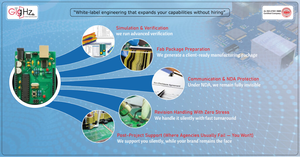
✔ Consistent delivery quality
✔ Zero hiring or overhead cost
✔ Fast turnaround
✔ Advanced engineering capabilities (SI, PI, Thermal, EMI)
✔ A complete engineering department behind your brand
You remain the hero to your client —
we just make you look stronger, faster, and more reliable.
Book a Call. Schedule a Free Consultation now. https://calendly.com/gighz/30min
Stuck in a loop of challenges? Always pick smart solution that works
Have you faced costly rework because 2D drawings skipped in MCAD workflows?
Effective way to prevent MCAD documentation errors recalls?
Please answer both poll questions before submitting.
Thank you for your response! 😊
Latest Post
Get Customized Engineering CAD Design Service

Book a Free Consultation Call
Partner with Gighz and bring your most innovative design concepts to life. Our engineering cad services accelerate development so you can focus on your big vision.
