When creating a PCB, each component should have its own distinct area in the board referred to as a PCB footprint Library.
The footprint defines the component’s physical placement, including pads, holes, and outlines.
An accurate footprint allows parts to fit properly, solder consistently, and the board operates correctly.
Altium Designer provides tools for creating, managing, and verifying footprints, allowing you to control pad shapes, dimensions, layers, and even 3D representations.
This enables the design procedure to become more accurate and reduces the potential for errors in production.
By the end of this tutorial, you will master the creation, structuring, and verifying footprints one-by-one in Altium Designer and construct a library enhancing design speed and reliability.
Understanding PCB Footprints in Altium
PCB footprints are the physical representation of the component onto the PCB.
It includes the pads for soldering pins, holes for through-hole components, and the placement outline.
They are related with schematic symbols, which identify the component electrically.
When you add a symbol in the schematic, it automatically assigns the right footprint in the layout so the electrical and physical design are consistent.
For instance, a schematic symbol for a resistor shall be paired with a resistor footprint on the board.
This connection prevents placement errors and lets your design be right from schematic all the way through board.
Why Footprint Accuracy Matters
Even minor mistakes in foot-print dimensions can lead to assembly issues.
The pads are too small in some instances, thus they may not solder well enough, the holes are misaligned, and wrong spacing can cause shorting.
Following the guidelines for IPC footprints (IPC-7351) supports the creation of reliable and manufacturable footprints.
They are used in defining the sizes, spacings, and tolerances in pads and designing precise footprints.
Accuracy allows parts to fit just right, perform consistently, and minimize production problems.
Before You Start Create a Footprint
Preparation is essential before starting footprint creation:
- Accumulate component datasheets: Confirm pin dimensions, pin spacing, package type, and mechanicals. Correct datasheet information is required for the correct foot print design.
- Decide the approach: You can create a footprint from scratch or use existing Altium libraries.
Altium also gives you a Content Vault and Manufacturer Part Search, and these have pre-made, verified footprints.
Using these can be a timesaver, but having specific footprints lets you have total control and precision.
- Keep mechanical restraints in mind: Consider board size, proximate parts, and thermal needs in order for the footprint to integrate well in the design.
Accurate preparation enables the smooth creation and minimal errors in layout and assembly.
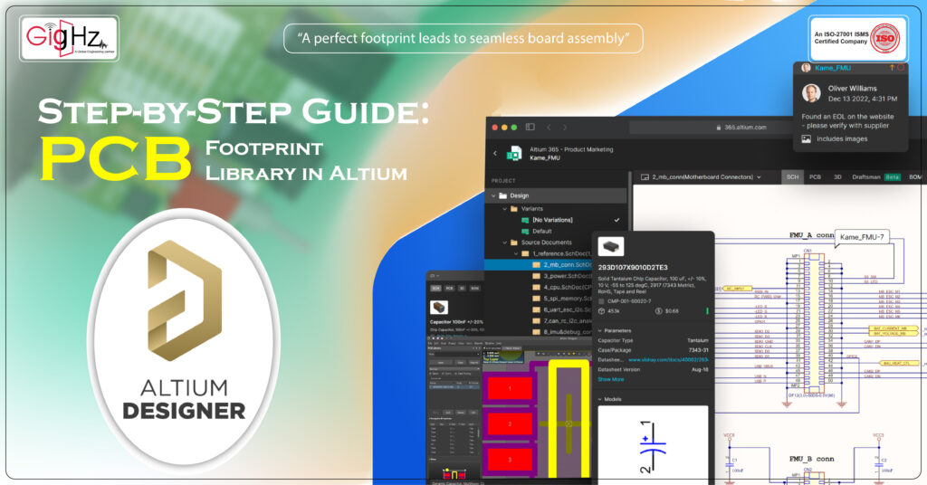
Step-by-Step guide: Creating a PCB Footprint in Altium Designer
Step 1: Open PCB Library Editor
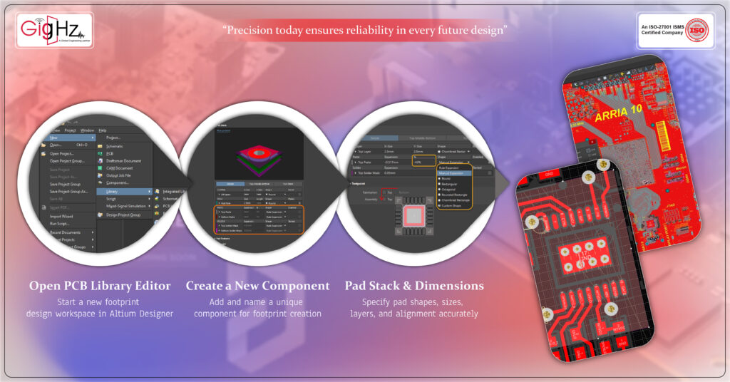
Begin with opening the PCB Library Editor in the Altium Designer from the menu item: File → New → Library → PCB Library. Here’s where all your footprints are going to reside.
When you invoke the editor, you should see the footprint panel, the main work area, and the layer controls.
The panel includes all the parts in the library, and the workspace is where you really sketch pads, outlines, and so forth.
Layer controls allow you to switch silkscreen, copper, or mechanical layers off and on.
It does take some time to get used to these features, but then you can work more quickly since you are moving and substituting footprints.
Step 2: Create a New Component
When the library editor pops up, click the “Add Component”. Name your new component in a descriptive and unique way, i.e., “SOIC-8”, and reference designator such as U1 or R1.
Be certain that you get the type correct.
Proper naming and correct type assignment can be considered insignificant, but they become very important when your library becomes large.
Without this, in large projects component searches are confusing and error-prone.
Think of this step as laying the foundation for organized library management.
Step 3: Define Pad Stack and Dimensions
Then add component pads. The component pads are where the electric contacts are actually made, so accuracy here becomes paramount.
For each mat, you should indicate:
- Pad shape: round, rectangular, or oblong
- Hole size (for the through-hole parts
- Layer stack: all, top, or base layers
- Plating: if the pad is through-hole plated oder Surface-mount
Synchronize the pad pitch, the width, and the height very accurately with the datasheet. Proper dimensions facilitate correct soldering, efficient connectivity, and effortless assembly.
One very small but useful tip here is to check the orientation of the pin and the pad with the schematic symbol.
This step avoids mapping errors that can lead to misalignment between your PC board layout and schematic later.
Step 4: Add Silkscreen and Courtyard Layers
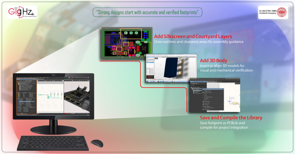
Once pads are specified, then the component must be defined in terms of silkscreen and courtyard layers.
Silkscreen shows the component outline and pin 1 orientation on the board, helping the assembly team identify components during soldering.
The courtyard layer defines a placement safety area around the part such that no overlap and no collision with other parts.
Such layers can seem nonfunctional when deposited, but play a crucial role in assembly precision and reproducible manufacturing.
Properly defined profiles also enable the automated assembly machines to have enough clearance and allow the human operator to recognize parts easily.
Step 5: Add 3D Body
To facilitate the visual effect, you can incorporate a 3D model or a simple 3D shape which stands in for the part.
Align the 3D body with mechanical drawings to verify its physical placement on the board.
This step becomes particularly useful in defining mechanical conflict, height clearance, or fit conditions that are less likely to be immediately obvious in 2D.
It enables you to see the component in the assembly layout at the component level, therefore eliminating assembly mistakes and rework.
Step 6: Save and Compile the Library
The right and verified PCB footprint library is the key to successful implementation of the PCB.
Exact footprints minimize assembly faults, maximize soldering consistency, and guarantee your board works the way it should.
By designing with caution, building the footprints in incremental stages, validating them, and keeping your library well-organized, you can establish a library of reusable parts that save you time, minimize errors, and foster collaboration.
Investing time in your footprint library upfront pays off in smoother PCB projects and more reliable designs.
Bottom Line
The right and verified PCB footprint library is the key to successful implementation of the PCB.
Exact footprints minimize assembly faults, maximize soldering consistency, and guarantee your board works the way it should.
By designing with caution, building the footprints in incremental stages, validating them, and keeping your library well-organized, you can establish a library of reusable parts that save you time, minimize errors, and foster collaboration.
Investing time in your footprint library upfront pays off in smoother PCB projects and more reliable designs.
Book a Call. Schedule a Free Consultation now https://calendly.com/gighz/30min
Stuck in a loop of challenges? Always pick smart solution that works
Have you faced costly rework because 2D drawings skipped in MCAD workflows?
Effective way to prevent MCAD documentation errors recalls?
Please answer both poll questions before submitting.
Thank you for your response! 😊
Latest Post
Get Customized Engineering CAD Design Service

Book a Free Consultation Call
Partner with Gighz and bring your most innovative design concepts to life. Our engineering cad services accelerate development so you can focus on your big vision.