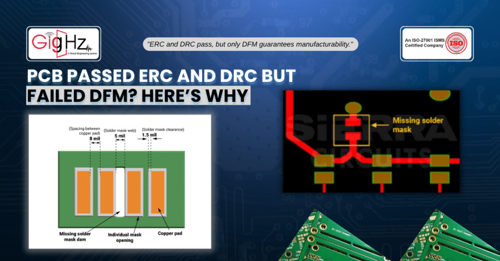
Now, your design passed ERC and DRC with no error!
Likewise, the layout looked clean, and the nets checked out fine.
Yet when the board went for fabrication, it failed the DFM in the PCB design stage.
Why?
Because ERC and DRC only validate electrical rules inside the ECAD tool.
They don’t account for how a factory will actually build your PCB.
So, that’s why so many teams run into PCB DFM check failure even when everything seems correct on-screen.
The gap between design rules and real-world manufacturing is where most problems occur.
If you don’t consider PCB manufacturability problems early, the result is costly redesigns, scrapped boards, and delays that no project manager wants to explain.
So let’s break down where things usually go wrong, and how following design for manufacturability guidelines PCB can prevent these issues from showing up at the very last stage.
1. Assuming ERC/DRC Means You’re Safe
So, passing ERC or DRC doesn’t guarantee manufacturability. But, these checks only validate what’s inside your tool’s logic — not the physical process your vendor uses.
Common DFM issues in PCB design include:
- Drill-to-copper clearances smaller than your fab shop can handle
- Trace widths that don’t match plating or etching tolerances
- Inadequate annular rings that lead to via reliability issues
- Keep ≥8 mil to meet typical fab capabilities and avoid shorts or etch violations.
- Maintain a ≥5 mil minimum to ensure reliable via plating and avoid breakout during fabrication.
The fix? Always align your PCB layout DFM rules with your manufacturer’s exact specs. Default ECAD constraints are generic and often too optimistic for real-world builds.
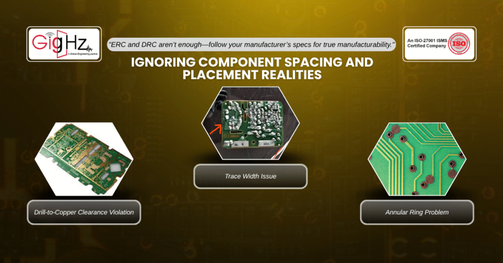
2. Ignoring Component Spacing and Placement Realities
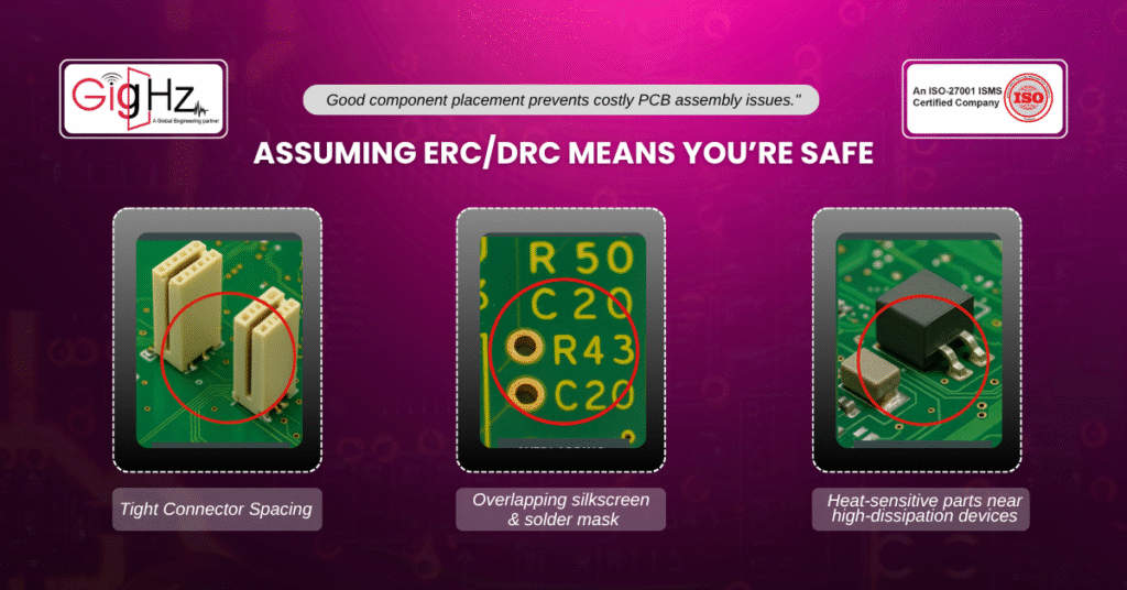
Plus, many PCB manufacturability problems show up not in the routing, but in how components are placed. Even if the layout looks correct, assembly becomes impossible if there isn’t enough space.
Watch for:
- Tight connector spacing that wave soldering can’t accommodate
- Overlapping silkscreen and solder mask leading to alignment errors
- Heat-sensitive parts placed next to high-dissipation devices
Following design for manufacturability guidelines PCB here avoids late-stage changes where moving even one part means re-routing half the board.
- Keep ≥100 mil between tall connectors for wave soldering, and ≥50 mil between BGAs and passives for safe rework.
- Maintain ≥1 mm solder mask clearance around pads to prevent bridging and improve solder reliability.
3. Treating Vias as Just Routing Convenience
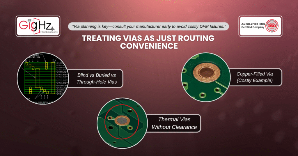
Now, Vias look simple in ECAD, but in fabrication they’re complex. Also, improper via planning is a major cause of PCB DFM check failure.
So, the issues often include:
- Blind or buried vias specified when the fab only supports through-holes
- Copper-filled vias designed without consulting about cost or feasibility
- Thermal vias missing clearance for soldering and assembly
When setting PCB layout DFM rules, involve your vendor early. Now, this way you’ll know which via types are realistic for your budget and timeline.
The Hidden Documentation Gap
Even if the layout is correct, missing or unclear documentation can trigger PCB manufacturability problems. Also, Gerbers without drill maps, incomplete assembly drawings, or vague stack-up notes leave fabricators guessing. And when they guess, the board you get may not be the one you designed.
So, think of documentation as part of the design for manufacturability guidelines PCB itself. So, every file you hand over should reduce ambiguity and increase predictability.
Leveraging AI to Bridge the DFM Gap
Now, bridging the gap between design and manufacturing can be daunting, however AI is increasingly helping to close it. Modern AI-driven PCB tools go beyond basic ERC and DRC by incorporating manufacturer-specific constraints, real-time DFM feedback, and predictive analytics. Also, these systems flag potential fabrication issues early—like drill tolerances, component spacing, and via feasibility—long before the design reaches the fab.
By integrating AI-assisted DFM checks into the design flow, engineers can avoid costly redesigns and accelerate time-to-market. The result is a smarter, more collaborative process where design intent and manufacturing realities align seamlessly. Ultimately, AI acts as a virtual manufacturing expert, catching hidden pitfalls and ensuring your PCB isn’t just functional, but also buildable and reliable from day one.
Why Vendor Alignment Is Non-Negotiable
Finally, one of the most underestimated reasons behind common DFM issues in PCB design is lack of early vendor communication. Every manufacturer has different tolerances, material availability, and process limits. If you don’t confirm these details upfront, even a “perfect” design can fail.
Good practice is to exchange your preliminary design with the fab house before tape-out. Their feedback often highlights DFM risks invisible to ERC or DRC. This step alone prevents many PCB manufacturability problems that derail projects later.
Final Word
Summing up, passing ERC and DRC is just the beginning, not the end. True design success comes from designing with manufacturability in mind — catching common DFM issues in PCB design before they become expensive production failures. By aligning PCB layout DFM rules with vendor capabilities, managing component spacing, treating vias strategically, and documenting thoroughly, you can eliminate most risks.
At Gighz, we’ve seen teams cut redesign cycles in half simply by adopting proper design for manufacturability guidelines PCB. Your boards not only work electrically but also get built right the first time.
So, If you want to ensure your next design clears every stage — from ERC to real-world manufacturing — reach out to us at info@gighz.net
Let’s make your next PCB a first-pass success.
Stuck in a loop of challenges? Always pick smart solution that works
Have you faced costly rework because 2D drawings skipped in MCAD workflows?
Effective way to prevent MCAD documentation errors recalls?
Please answer both poll questions before submitting.
Thank you for your response! 😊
Latest Post
Get Customized Engineering CAD Design Service

Book a Free Consultation Call
Partner with Gighz and bring your most innovative design concepts to life. Our engineering cad services accelerate development so you can focus on your big vision.