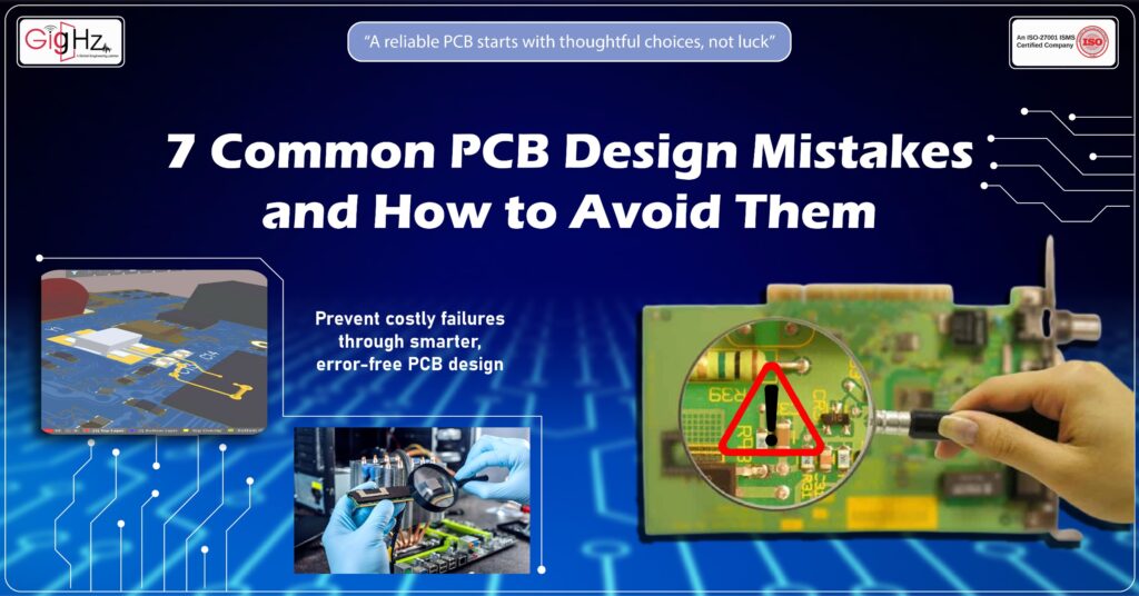
Finishing a PCB design always feels good.
You see the layout on your screen, and everything seems in place.
But the real challenge begins once the board is manufactured.
That’s often when hidden mistakes show up—sometimes small, but costly enough to cause failure.
The tricky part is that most problems don’t come from advanced engineering issues.
They usually come from simple oversights: a component placed too close, a trace that’s too thin, or heat that isn’t managed properly.
These small details can quietly decide whether your design works as expected or fails in testing.
The good thing is, you can prevent most of these issues.
By paying attention to common mistakes and making careful choices early on, you can save time, reduce costs, and build boards that work reliably from the start.
Now, let’s look at the most common PCB design mistakes—and how you can avoid them before sending your board to manufacturing.
1. Poor Component Placement
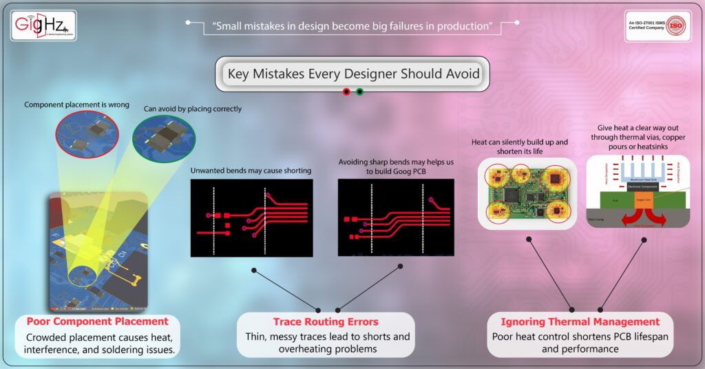
Let’s start with something that sounds simple but causes endless issues—component placement.
Many designers get so focused on fitting everything within the board size that they forget how those components will interact.
Place them too close together, and you invite soldering difficulties, heat buildup, or even electrical interference.
How to avoid it:
Before you drag and drop parts onto the layout, pause and think about the natural flow of your circuit.
Power components should sit close to the power inputs.
High-speed digital signals should stay away from sensitive analog sections.
Heat-generating components should have sufficient clearance from neighboring parts and traces to allow effective thermal dissipation.
Consider the PCB as an integrated system, where component placement affects both electrical performance and thermal management.
Allocating proper space during the layout stage helps prevent overheating, reduces thermal stress on components, and minimises potential reliability issues in operation.
2. Trace Routing Errors
Once the components are in place, the next challenge is routing traces.
Think of traces as the highways of your PCB design mistakes—they carry the signals and power that keep everything alive.
But if they’re too thin for the current they carry, placed too close to one another, or routed with unnecessary bends, they can cause shorts, crosstalk, overheating—these problems often come down to routing mistakes.
How to avoid it:
First, figure out how much current each trace will carry and make the trace wide enough to handle it safely.
Keep enough space between traces so they don’t accidentally touch or interfere with each other.
For important signals, try to keep the traces straight and avoid sharp bends—this helps the signal travel cleanly without distortion.
Paying attention to these details now makes your PCB more reliable and reduces problems later.
3. Ignoring Thermal Management
Now, let’s talk about something that’s easy to overlook because you can’t always see it—heat.
A board might look perfect on your desk at room temperature, but once it’s inside an enclosure, heat can silently build up and shorten its life.
Many PCBs fail not because of poor circuits, but because thermal management was ignored.
How to avoid it:
Start by identifying which components generate the most heat.
Then, give that heat a clear way out—through thermal vias, copper pours, or heatsinks.
Don’t just assume the board will “be fine.” Use simulations or at least simple calculations to estimate temperatures.
Heat management isn’t an optional extra; it’s essential if you want your design to survive in real-world conditions.
4. Overlooking Signal Integrity
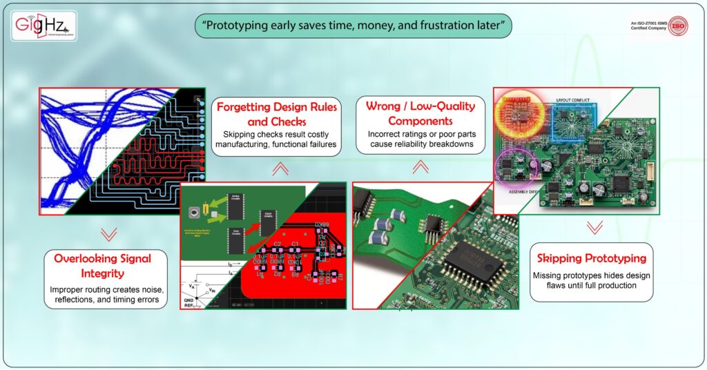
As circuits get faster and more complex, signal integrity becomes critical.
Noise, reflections, or timing errors can cause the board to stop working correctly.
Many designers focus only on the layout—where parts go, how traces look—without considering how signals physically behave as they travel.
How to avoid it:
Keep differential pairs tightly coupled.
Separate analog and digital signals so they don’t interfere with each other.
Use proper impedance matching for high-speed traces to avoid reflections.
If possible, run quick simulations to visualize how your signals behave before you send the board for manufacturing.
Think of your signals as messengers again—if the roads are messy or full of detours, the message won’t arrive intact.
Clear, uninterrupted paths make all the difference.
5. Forgetting Design Rules and Checks
When the design looks almost finished, excitement often takes over.
That’s when it’s easy to overlook something important: design rules.
Skipping checks might not feel like a big deal in the moment, but it can lead to boards that either can’t be manufactured or fail immediately after.
How to avoid it:
Use the tools already built into your CAD software.
Run design rule checks (DRC) and electrical rule checks (ERC).
They act as your safety net, catching mistakes you might not see when you’re too close to the project.
Think of them as a friend who reviews your work and says, “Hey, you missed this.” A few minutes of checking can prevent weeks of wasted effort.
6. Using Wrong or Low-Quality Components
Here’s another one that’s more common than most designers admit: component selection.
You can have the perfect layout, but if you pick the wrong component—or a low-quality one—your board will fail.
Wrong ratings, mismatched tolerances, or even an incorrect footprint can stop a project in its tracks.
How to avoid it:
Always double-check.
Verify that your component’s footprint in the software matches the real part.
Make sure ratings and tolerances align with your circuit’s needs.
And whenever possible, source components from reliable suppliers.
7. Skipping Prototyping
PCB mistakes are more common than many realise, but they don’t have to derail your project.
By placing components thoughtfully, routing traces carefully, managing heat, preserving signal integrity, checking rules, choosing the right components, and prototyping, you can prevent most problems before they ever reach the factory floor.
At its core, PCB design mistakes is both technical and thoughtful. Every choice—trace width, component position, thermal path—shapes how well the board performs.
With attention, care, and foresight, you can avoid frustration, save costs, and build a board that works reliably the first time.
The goal isn’t just to finish a PCB—it’s to finish it well. Mistakes may carry lessons, but with careful design and good habits, many of them don’t need to happen at all.
Bottom Line
Summing up, skipping drawings isn’t a fast process but a very risky one to avoid.
Likewise, skilled MCAD teams always build and make room for 2D drawing standards into their workflows from day one itself.
Truly, 3D modeling covers approximately 90% of the entire design process!
But, it solely cannot close the final 10% required to optimal standards,
Therefore, detailed 2D drawings are always essential and highly needed to bridge that gap.
That’s why, we help engineering teams across industries to upgrade their MCAD workflows with bulletproof 2D documentation.
Likewise, our experts identify the drawing gaps, tolerance stack-up oversights, and compliance weak spots for you – as a result, you get tested templates and smart review flows.
Follow us on LinkedIn for faster updates https://www.linkedin.com/in/chandra-thimma/recent-activity/all/
Stuck in a loop of challenges? Always pick smart solution that works
Have you faced costly rework because 2D drawings skipped in MCAD workflows?
Effective way to prevent MCAD documentation errors recalls?
Please answer both poll questions before submitting.
Thank you for your response! 😊
Latest Post
Get Customized Engineering CAD Design Service

Book a Free Consultation Call
Partner with Gighz and bring your most innovative design concepts to life. Our engineering cad services accelerate development so you can focus on your big vision.