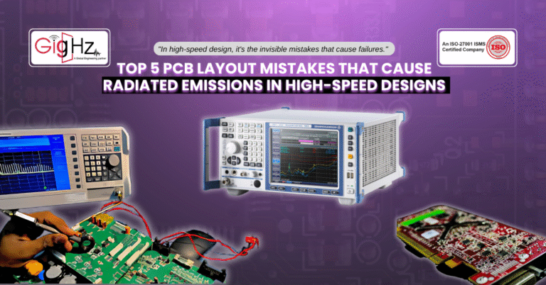
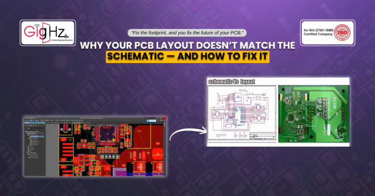
So, you must have optimised the schematic, chosen the right components, and even double-checked stack-up rules.
But when the board...
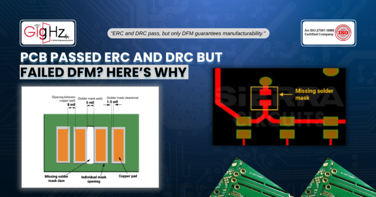
Now, your design passed ERC and DRC with no error!
Likewise, the layout looked clean, and the nets checked out fine.
Yet when the...
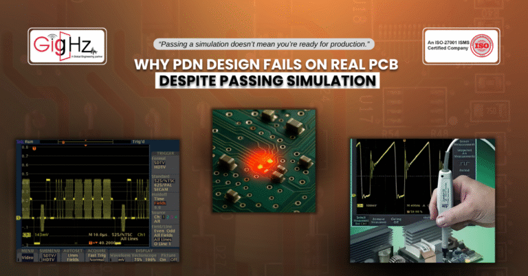
So, apparently, you must have run all the simulations, where everything looks stable, and the margins seem completely safe.
But when...
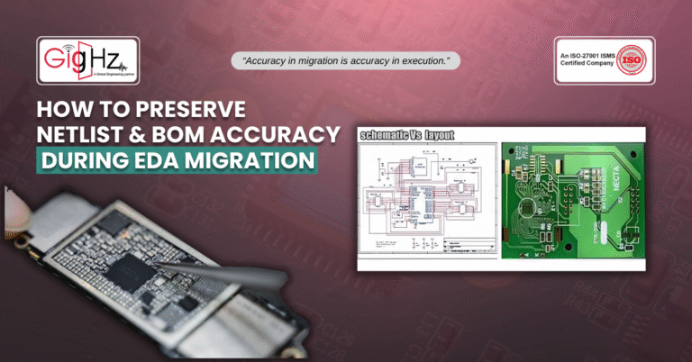
As we all know, it goes without saying that switching ECAD platforms is never as simple as clicking “export” and “import.”
Yes,
If...
So, you have double-checked your design, right?
Likewise, the schematic is clean, ERC passed, and you are feeling confident. But when...
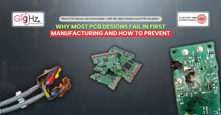
Nearly 70% of new PCB designs fail in their very first manufacturing run.
Yes, engineers invest weeks of effort into schematics and...