Why Are HDI PCB Revolutionizing Compact Designs in Today’s Cars?
- Posted On:
- October 15, 2024
- Category:
- Ecad

HDI PCB
As technology gets more complex, hardware is getting much smaller.
HDI PCBs provide many benefits, including fitting more connections into smaller spaces.
This allows for smaller circuit boards that can be used in various applications.
Your computers are now much lighter, so you can work on your laptop and manage your business while traveling.
Plus, you can enjoy watching your favorite movies on your smartphone during your flight.
As cars become more advanced, the role of the infotainment system has expanded significantly.
One of the key components of this system is the display touchscreen control module, which relies heavily on High-Density Interconnect (HDI) PCBs.
Modern cars are packed with technology, and space is limited, especially for the infotainment system’s control module.
HDI PCBs use multiple layers to fit more circuitry into a smaller area.
This is essential for the compact design of display touchscreen control modules.
Their compact design, enhanced signal integrity, efficient power distribution, effective thermal management, and support for advanced features make them essential for integrating complex electronics into automotive infotainment systems.
As cars continue to evolve, HDI PCBs will remain pivotal in advancing automotive technology and improving the user experience.
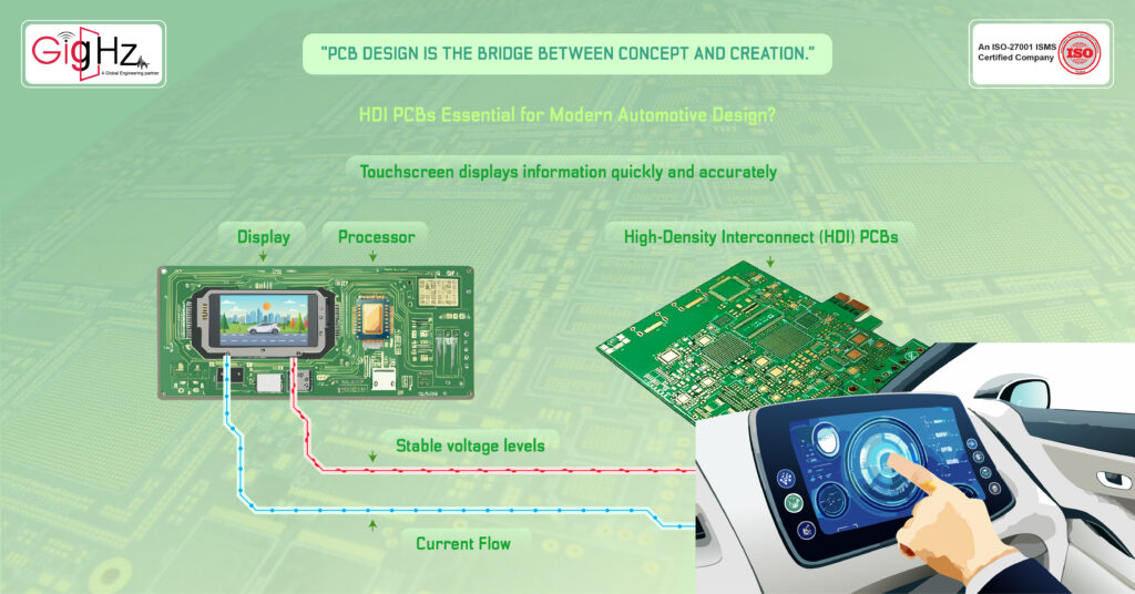
What Makes HDI PCBs Essential for Modern Automotive Design?

In today’s vehicles, touchscreen displays are integral to the driving experience, providing both functionality and aesthetic appeal.
For these displays to work effectively, they must process information quickly and accurately while fitting into a sleek, compact design.
High-Density Interconnect (HDI) PCBs are crucial in achieving this balance.
Here’s a continuous look at why HDI PCBs are essential for modern automotive design:
Current is the flow of electric charge through a circuit, powering the touchscreen and enabling its functions.
When you touch the screen, sensors detect the touch by measuring changes in the current flow.
This data is transmitted through the PCB to the processor, which interprets your input and adjusts the display accordingly. The fine line traces on HDI PCBs ensure that current flows correctly, maintaining a responsive and accurate touchscreen.
Voltage is the electrical pressure that pushes the current through the circuit, crucial for the touchscreen’s response to inputs.
Stable voltage levels are essential for the touchscreen to process inputs correctly.
Any fluctuations in voltage could result in slow response times or inaccuracies. HDI PCBs prevent these issues by maintaining consistent voltage, ensuring that every touch is registered accurately and promptly.
Power is the product of voltage and current, representing the energy required to keep the touchscreen module operational.
For the touchscreen to function properly, it needs a stable and efficient power supply.
HDI PCBs manage this by ensuring that power is evenly distributed and by incorporating features to prevent overheating.
This allows the touchscreen to perform reliably without draining the car’s battery or causing thermal issues.
Why Are HDI PCB Revolutionizing Compact Designs in Today's Cars?

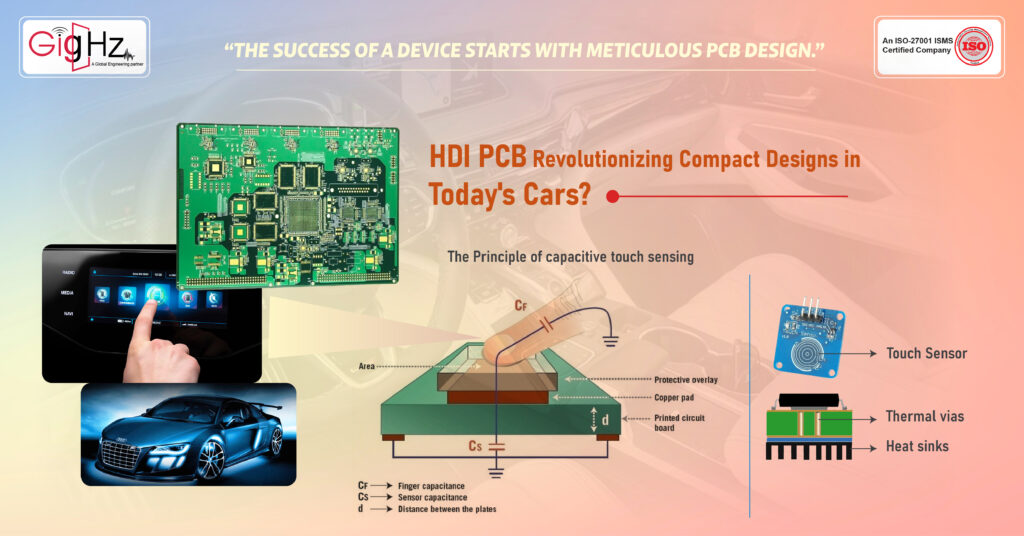
HDI PCBs play a crucial role in modern automotive touchscreen modules by managing electrical signals, power, and heat to ensure optimal performance. They route electrical signals from the touchscreen sensors to the control processor through multiple layers. This routing is essential for handling different types of signals, such as touch inputs and display data. When a user interacts with the touchscreen, sensors detect touch coordinates and transmit this data through the PCB’s signal paths to the processor, which then adjusts the display accordingly. Precise signal routing ensures that touch inputs are accurately detected and processed, providing a responsive user interface.
Power distribution is also managed through dedicated power planes within the HDI PCB. These planes are designed to deliver electrical power to various components, including the display, touch sensors, and processing units. Proper power management ensures that each component receives the correct amount of energy, maintaining stable operation and preventing power fluctuations that could affect performance.
Voltage regulation is another critical function of HDI PCBs. They include voltage regulators and filters to stabilize the voltage supplied to different parts of the touchscreen module. This consistent voltage is crucial for the proper functioning of the display and touch sensors, preventing issues such as screen flickering or unresponsive inputs.
Thermal management is addressed through the use of thermal vias and heat sinks incorporated into HDI PCBs. These components work to transfer heat away from sensitive areas, preventing overheating and maintaining performance and reliability. Effective thermal management enhances the durability of the touchscreen module, ensuring it performs well over the vehicle’s lifespan.
Overall, HDI PCBs use advanced layering, Microvias, and fine traces to integrate high-performance components into a compact space. This design allows for efficient routing of signals and power while managing heat effectively, ensuring that modern automotive touchscreen modules operate with high efficiency, quick response times, and stable performance.
HDI PCB design tips

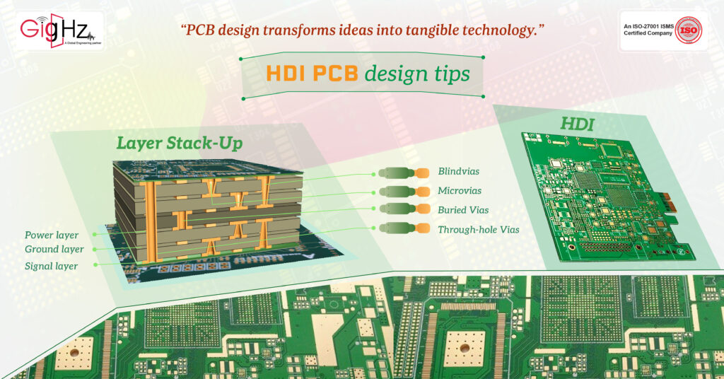
Optimize Layer Stack-Up
- Use a balanced layer stack-up for signal integrity.
- Pair signal layers with adjacent ground or power planes.
Utilize Microvias
- Implement microvias to enable high-density interconnections.
- Reduce via footprint to save space and improve signal integrity.
Incorporate Blind and Buried Vias
- Use blind vias for connecting outer layers to inner layers.
- Utilize buried vias for internal layer interconnections without penetrating outer layers.
Design for Signal Integrity
- Route high-speed signals between closely paired ground and power planes.
- Minimize via transitions and use impedance-controlled traces.
Implement Advanced Routing Techniques
- Use fine line traces and spaces to increase routing density.
- Optimize trace widths and spacings according to signal frequency and impedance requirements.
Manage Power Distribution
- Design dedicated power planes to ensure stable voltage supply.
- Integrate decoupling capacitors close to power pins to minimize noise.
Enhance Thermal Management
- Use thermal vias and heat sinks to dissipate heat effectively.
- Implement copper pours and heat spreaders to distribute heat across the PCB.
Ensure Proper Via Placement
- Strategically place vias to minimize signal path lengths and reduce inductance.
- Avoid excessive via use to prevent signal degradation.
Incorporate Effective Grounding
- Design solid ground planes to reduce noise and interference.
- Ensure continuous grounding for high-frequency signal paths.
Verify Design with Simulation Tools
- Use simulation tools for signal integrity, thermal analysis, and power distribution.
- Validate design performance under operational conditions before production.
Final Thoughts
In conclusion, the evolution of pcb design has significantly advanced with the introduction of high density interconnect (HDI) technology. The use of HDI printed circuit boards allows for a higher wiring density, enabling manufacturers to create more compact and efficient electronic devices.
The manufacturing process of HDI PCBs involves intricate techniques such as microvia technology and careful lamination processes, which facilitate the interconnection of printed circuit layers, ensuring that the pcb material is utilized effectively.
The design rules associated with HDI board design allow for multiple layers of the PCB to be integrated seamlessly, resulting in reduced space requirements and improved performance. The advantages of HDI include enhanced signal integrity and reduced weight, which are crucial for modern electronic applications.
As we continue to explore different types of HDI, the HDI manufacturing process will become increasingly vital in the realm of pcb fabrication and pcb manufacturing, paving the way for innovative solutions in the electronics industry.
To know more insights, reach our experts,
Schedule a Call. Book a free consultation now. https://calendly.com/gighz/30min
Table of Contents
Latest Post
Get Customized Engineering CAD Design Service

Book a Free Consultation Call
Partner with Gighz and bring your most innovative design concepts to life. Our engineering cad services accelerate development so you can focus on your big vision.
