How My Biggest Mistakes in EV PCB Design Led to Valuable Lessons?
- Posted On:
- December 3, 2024
- Category:
- Ecad

PCB Design Mistakes
There’s a saying in the world of engineering,
“You don’t truly learn something, until you break it”.
As the PCB design companies, the goal is to walk away from your mistakes with your career intact.
With 30+ years of design experience behind me,
As a professional specializing in PCB design for the automotive sector,
I’ve encountered a variety of challenges, from balancing signal integrity to managing the growing demand for smaller, more efficient designs.
The complex aspects have been working with evolving technologies like EVs, where power efficiency and reliability are paramount.
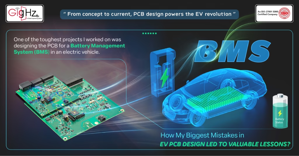
One of the toughest projects I worked on was designing the PCB for a Battery Management System (BMS) in an electric vehicle.
The task required meticulous attention to detail, particularly around thermal management and power distribution.
Initially, I underestimated how much space was needed for heat dissipation.
What I thought was a minor oversight turned into a major issue, taught me valuable lessons that have since guided my approach to every new project.
Here’s a look at that experience and the key takeaways I gained from it.
How My Biggest Mistakes in EV PCB Design Led to Valuable Lessons?

One of the most significant mistakes I made in EV PCB design came when I underestimated the importance of thermal management in high-power circuits, in Battery Management Systems (BMS).
The BMS is responsible for monitoring the health of the battery pack, ensuring that the battery cells are charged and discharged optimally to avoid thermal runaway or overvoltage conditions.
This requires precise power distribution, fault-tolerant designs, and above all, effective thermal management.
When designing the PCB for a BMS, I initially focused too heavily on component density and signal integrity—prioritizing the miniaturization of the design and signal routing for communication between sensors, microcontrollers, and power devices.
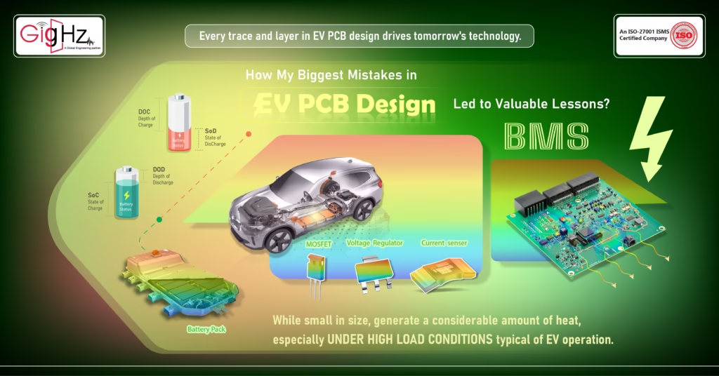
What I failed to account for, however was the power dissipation from key components like MOSFETs, voltage regulators, and current sense resistors. These components, while small in size, generate a considerable amount of heat, especially under high load conditions typical of EV operation.
In my initial design, I placed these components too close together, assuming that the existing thermal vias would be sufficient to handle heat dissipation.
As a result, when we tested the prototype under real-world conditions, the PCB quickly overheated, leading to thermal throttling and eventually component failure.
This not only caused system instability but also required a complete redesign of the thermal management system, adding significant cost and delays to the project timeline.
Lessons Learned: Thermal Management and Component Placement in PCB

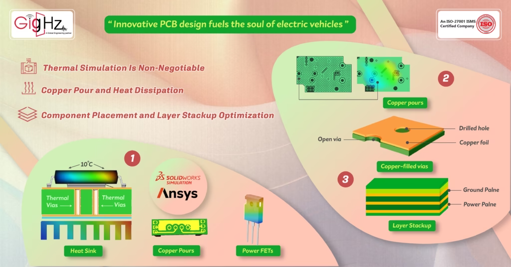
1. Thermal Simulation Is Non-Negotiable
One of the first lessons I learned from this mistake was the importance of thermal simulations.
Early on, I had relied on basic simulations for signal integrity and power distribution, but I had overlooked detailed thermal analysis.
After this experience, I began using more advanced thermal simulation tools such as ANSYS and SolidWorks Flow Simulation to predict the thermal behavior of the PCB under varying load conditions.
These tools allow you to model heat sources, evaluate thermal vias, and simulate airflow in enclosures.
They also help identify hot spots in the design where additional heat sinking or copper pours are required.
After using thermal simulations on my next BMS design, I was able to reposition the power FETs and voltage regulators to more thermally optimal locations.
This not only improved heat dissipation but also made the design more compact without compromising thermal performance.
2. Copper Pour and Heat Dissipation
In my earlier designs, I missed the power of copper pours in aiding heat dissipation.
When designing for power applications in EVs, thermal vias are essential to transfer heat from hot components to other layers of the PCB. However, copper pours—large continuous copper areas connecting ground planes and power traces—can also significantly improve thermal management. By increasing the copper area in high-power sections of the PCB, heat can be spread more efficiently across the board, reducing hotspots.
On my second attempt at the BMS PCB, I used a more aggressive copper pour strategy, including high-current ground pours and copper-filled vias to ensure heat was conducted efficiently across the PCB. This allowed me to achieve a more balanced thermal distribution, lowering component temperatures by more than 10°C, which improved system stability and longevity.
3. Component Placement and Layer Stackup Optimization
Another lesson I learned the hard way was the importance of component placement in relation to thermal dissipation and electromagnetic interference (EMI).
In my initial design, I had placed the high-power components next to sensitive low-voltage signal traces, leading to cross-talk and signal degradation due to thermal effects and EMI.
After analyzing the prototype’s failures, I adopted a more structured approach to component placement. I began to prioritize thermal zones, where high-power components were placed on inner layers of the PCB, away from sensitive components.
This also led to better signal integrity, as the routing of high-speed signals was isolated from high-power components, reducing noise and interference.
In terms of layer stackup, I optimized the use of power planes and ground planes to ensure a solid reference for high-current traces.
I also added decoupling capacitors at key locations to smooth out voltage spikes that could have been caused by power distribution issues.
The Bigger Picture: Designing for Electric Vehicle (EV) Reliability and Efficiency

After this experience, I understood that designing PCBs for EVs is for more complex than simply routing traces and choosing the right components.
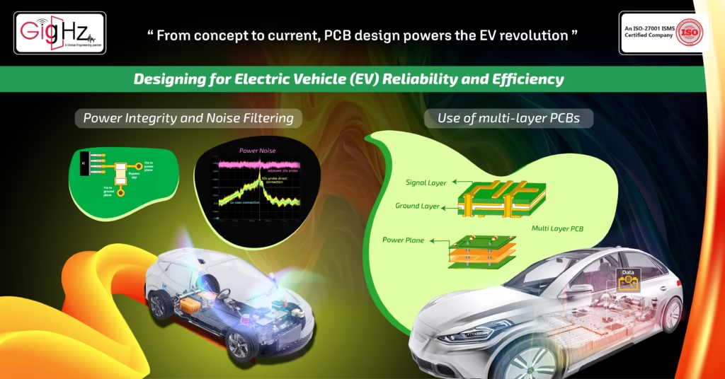
1. Power Integrity and Noise Filtering
In subsequent designs, I learned the importance of designing for power integrity.
Ensuring that your PCB handles power fluctuations without affecting the performance of sensitive circuits is crucial, especially in the case of high-voltage battery systems and motor controllers.
I began incorporating power decoupling capacitors, bulk capacitors, and low-inductance ground planes to ensure that the power distribution network was robust.
I also paid special attention to minimizing ground bounce and voltage spikes, using techniques like star grounding and controlled impedance traces to keep noise to a minimum.
2. Use of multi-layer PCBs
The high-density, high-power nature of EV systems often demands multi-layer PCBs to manage the complexity of the design. In my redesigns, I transitioned from simple two-layer designs to four-layer PCBs, with dedicated power planes and signal layers.
This allowed me to better isolate the power circuitry from sensitive signals while providing more room for thermal management features like vias and copper pours.
Final thoughts
Moreover, the benefits of using PCBs extend beyond mere functionality; they facilitate improvements in the transportation sector by enabling faster and more efficient EV charging.
As electric vehicles become a more viable option for drivers, the pcb industry must continue to innovate to ensure that the system’s longevity and performance are upheld.
The future of electricity in our daily lives is intertwined with the advancements in electronic manufacturing.
Unlock the Secrets to Better EV PCB Design – Get Expert Tips Delivered to Your Inbox! info@gighz.net
What’s been your biggest design challenge?
Let’s continue the conversation in the comments.
Latest Post
Get Customized Engineering CAD Design Service

Book a Free Consultation Call
Partner with Gighz and bring your most innovative design concepts to life. Our engineering cad services accelerate development so you can focus on your big vision.
