How to Learn PCB Design: A Simple Guide for University Startups
- Posted On:
- February 23, 2026
- Category:
- Ecad
For a university startup, learning PCB design is often the point where ideas start becoming real products.
Many teams can build quick prototypes on breadboards, but the moment they need a stable, compact, and manufacturable board, the process becomes confusing.
PCB design feels difficult not because of the software, but because most teams don’t know the correct learning path.
A PCB is the physical version of your circuit logic.
To design it well, students must understand electronics, create accurate symbols and footprints, build a clear schematic, follow layout rules, and prepare proper output files for manufacturing.
When even one step is skipped, the final board fails — either electrically, mechanically, or during assembly.
This guide gives university startups a simple, structured roadmap to how to learn PCB design from the ground up.
It explains exactly what to focus on at each stage, so your team can move from concept to a working board with fewer mistakes and more confidence.
1) Start With the Basics of Electronics
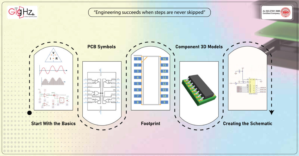
Before opening any PCB tool, a team must understand how electronic components work. Without this foundation, even the best PCB software cannot help.
Key points a startup should learn:
- Current, voltage, resistance, and power — how they interact
- Ohm’s law — simple but essential
- How components behave — resistors, capacitors, inductors, diodes, transistors
- Analog vs digital signals
- Reading a schematic — symbols, nets, reference designators
This helps the team understand why a PCB is not just “lines and shapes” but a physical form of an electrical idea. Once the basics are clear, the software becomes easier, and mistakes reduce drastically.
2) PCB Symbols: The Logical View
The first step in any PCB design tool is the creation or selection of symbols. A symbol is not a physical shape. It is a logical representation of a component used in the schematic.
A good symbol has:
- clear pins
- correct pin names and numbers
- readable labels
- logical grouping of pins (e.g., power pins together)
University teams often mix symbols from different libraries, leading to errors later. The best practice is:
- use a clean library
- verify every symbol with the component datasheet
- maintain naming consistency
A correct symbol ensures clean schematics and error-free connections.
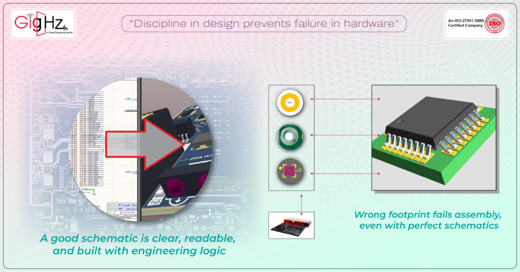
3) Footprint: The Physical View
After selecting the symbol, the next step is the footprint, which represents how the component sits on the PCB.
A footprint defines:
- pad size and shape
- pitch
- courtyard
- solder mask
- mechanical constraints
Without the correct footprint, the PCB will fail during assembly, even if the schematic is perfect.
University startups must learn:
- how to match footprint pin numbers with symbol pin numbers
- how to check the recommended land pattern in the datasheet
- how to set clearances and pad sizes according to fabrication limits
This teaches them the practical side of PCB design — how a board gets physically soldered.
4) Component 3D Models: Visual and Mechanical Fit
A 3D model helps students understand how the board looks in real life. It also helps avoid mechanical errors like component height issues or connector misalignment.
A good 3D model helps in:
- enclosure design
- checking collisions
- visualizing board density
- verifying connector directions
Most PCB tools allow importing 3D STEP models or assigning default shapes. University teams should develop the habit of viewing their design in 3D early in the process.
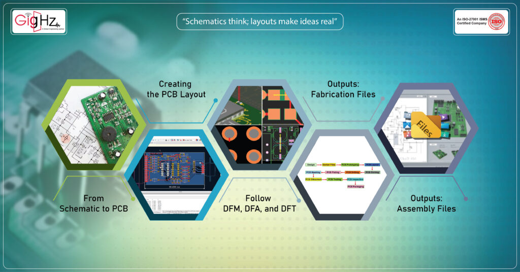
5) Creating the Schematic
Once symbols, footprints, and 3D models are ready, the team builds the schematic. A good schematic is clear, readable, and built with engineering logic.
Important practices:
- group functional blocks (power, microcontroller, sensors, communication)
- use net labels instead of long lines
- add notes and values
- add decoupling capacitors near ICs
- ensure power rails are consistent
- verify pin mapping carefully
Schematic creation is the stage where the actual “design thinking” happens. It is where the product’s brain takes shape.
6) From Schematic to PCB: Engineering Change Order (ECO)
When the schematic is ready, the designer pushes the data to the PCB layout — this process is usually called Engineering Change Order (ECO) or Synchronize Changes.
This step creates:
- component placement list
- net connectivity
- design rules
University students must understand that ECO is not a one-time step. Every change in schematic must be synchronized again. This builds discipline and prevents mismatched designs.
7) Creating the PCB Layout
Now the real physical design begins.
- a) Component Placement
Start with:
- connectors at edges
- high-speed parts close to each other
- power section in one corner
- microcontroller in the center
- decoupling capacitors close to IC pins
This sets a strong base for routing.
- b) Routing
Basic routing rules:
- use short traces
- keep power traces thicker
- maintain spacing
- avoid 90-degree bends
- use vias wisely
- maintain ground return paths
- separate analog and digital areas
A clean layout reduces noise, avoids heat problems, and improves reliability.
8) Follow DFM, DFA, and DFT
A student team must learn that PCB design is not only electrical. It must be manufacturable, assemblable, and testable.
DFM (Design for Manufacturing)
Ensures fabricators can build the board smoothly:
- correct trace widths
- spacing as per PCB vendor
- clean pad-to-pad distance
- avoid tiny copper joints
DFA (Design for Assembly)
Helps during soldering and assembly:
- aligned components
- correct polarity markings
- avoid too-tiny footprints
- place test points
DFT (Design for Testing)
Helps during debugging and validation:
- add test pads
- breakout important nets
- keep space around connectors
- label signals clearly
These principles reduce cost and prevent repetitive redesigns.
9) Outputs: Fabrication Files
When the layout is complete, the next step is generating outputs for the fabricator. These usually include:
- Gerber files
- drill files
- board outline
- stack-up details
- solder mask and paste layers
Fabricators use these files to create copper layers, apply solder mask, drill vias, and prepare the board.
10) Outputs: Assembly Files
For assembly, generate:
- Bill of Materials (BOM)
- Pick-and-place file
- 3D PDF or STEP
- assembly drawings
- polarity markings
These outputs help assemblers place components correctly, reducing rework.
Bottom Line
Learning PCB design is a journey that blends theory, tools, and practical thinking.
For university startups, the goal is not only how to learn PCB design a working board but to understand each stage of the process — from electronics basics to final manufacturing outputs.
When students learn symbols, footprints, 3D models, schematic creation, ECO flow, layout rules, DFM/DFA/DFT, and output files carefully, they build a strong foundation for future product development.
Mastering this process early gives a startup the confidence to convert ideas into real hardware — faster, cleaner, and with fewer mistakes.
Book a Call. Schedule a Free Consultation now. https://calendly.com/gighz/30min
Stuck in a loop of challenges? Always pick smart solution that works
Have you faced costly rework because 2D drawings skipped in MCAD workflows?
Effective way to prevent MCAD documentation errors recalls?
Please answer both poll questions before submitting.
Thank you for your response! 😊
Latest Post
Get Customized Engineering CAD Design Service

Book a Free Consultation Call
Partner with Gighz and bring your most innovative design concepts to life. Our engineering cad services accelerate development so you can focus on your big vision.