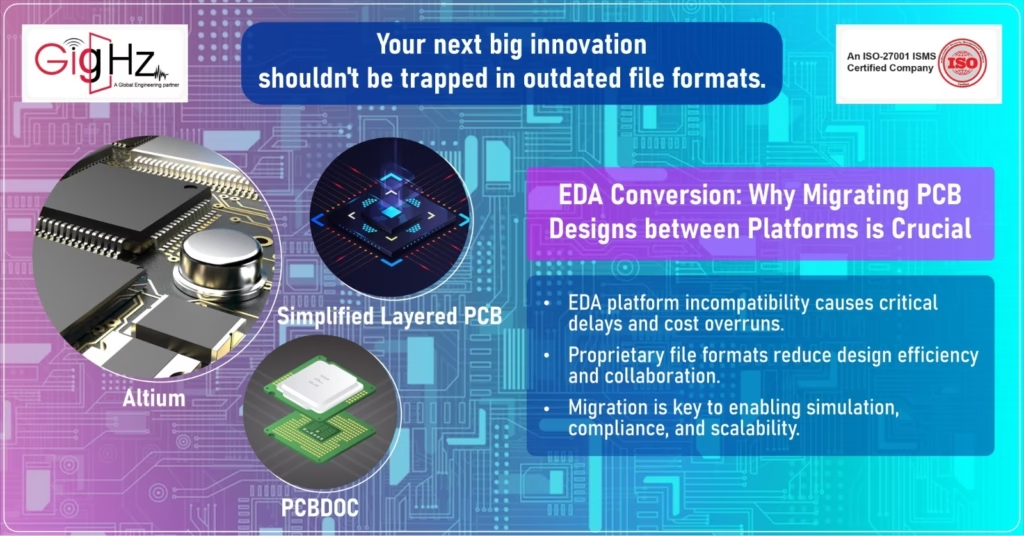
EDA Conversion: Why Migrating PCB Designs between Platforms is Crucial
- Posted On:
- June 25, 2025
- Category:
- Ecad
The electronics industry depends on innovation to develop faster, smaller and more capable devices.
The rapid technological progression faces a continuous obstacle because Electronic Design Automation (EDA) platforms cannot exchange PCB designs easily with each other.
The transfer of projects between different tools leads engineers to face expensive time delays and data damage plus software incompatibility problems.
The issues go beyond minor interruptions because they create significant delays that affect project schedules, budget spending, and final product operational capabilities.
The core functionality of contemporary electronics design rests on EDA technology, yet proprietary file standards plus specialized tool interfaces create isolated design environments that reduce both efficiency and collaboration abilities.
The conversion process between different platforms and vendors determines how successful a project will become or how it will fail.
In this tech-driven world where miniaturization is at its peak, PCB designers need to master EDA Technology conversion to stay competitive.
The True Cost of Platform Incompatibility

The electronic design automation industry faces severe fragmentation because Altium Designer, Cadence OrCAD, and KiCAD maintain their own separate file standards and design approaches.
Standardization deficiencies cause major migration obstacles.
According to an IEEE industry, study file conversion and compatibility troubleshooting problems cost engineering teams more than two weeks per project.
The production timeline suffers from these delays, which create both higher expenses and resource depletion for the team.
The process of conversion introduces delicate errors through component footprint misplacement and layer definition corruption and netlist errors which remain undetected until physical prototyping or testing phases trigger expensive redesigns.
The success of EDA migration affects organizational capabilities for growth, their capacity to meet compliance standards, and develop innovative solutions.
The implementation of advanced technologies by companies exposes gaps in older design tools such as sophisticated thermal analysis or signal/power integrity simulations, which lack necessary capabilities.
The process of platform advancement goes beyond convenience because it ensures design sustainability within advanced technological environments.
EDA Conversion: A Comprehensive Guide to Migrating PCB Designs between Platforms

The process of moving PCB designs between Electronic Design Automation (EDA) platforms requires careful execution and planning because it presents significant challenges. Engineers typically need such transfers when they update their tools or optimize their workflows or work with different software platforms.
The quality of a migration project execution determines the occurrence of design errors, project delays and additional expenses.
This guide outlines an in-depth methodical process which guarantees error-free transitions between different EDA technology platforms.
1. Establishing precise objectives and requirements.
Successful electronic design automation requires engineers to define both the migration necessity and the expected outcomes right from the beginning.
Engineers need to determine the primary reasons behind moving, since advanced EDA simulation capabilities, cost reduction or better collaboration features could serve as the drivers.
The requirements of each design team determine their need for specific EDA tools since high-frequency PCB designers need top-tier signal integrity analysis while those working with mechanical CAD need seamless integration.
The assessment process needs to analyze how files will exchange data between the existing system and the new target platform.
The exclusive file formats of Altium Designer’s .PcbDoc and Cadence Allegro’s .brd cannot be directly read by other software tools, which require converting files through intermediate formats.
The documentation of requirements at the beginning of the project avoids unexpected problems which could appear during later development.
2. Conducting a Comprehensive Design Audit
A thorough examination of the present PCB design should be performed before starting the migration process. A thorough review of schematic and layout files must happen to identify any problems with unrouted nets, floating components, and unresolved design rule violations. All discovered inconsistencies need resolution to achieve a smooth transition process.
The migration process requires special attention to custom design rules, which includes impedance control settings, differential pair routing, and high-speed constraints. The rules between EDA tools tend to differ, thus requiring post-migration manual adjustments. The verification of component libraries requires thorough examination because footprints symbols and supplier part numbers must match exactly to prevent mismatches between the old and new environments.
Design file backup stands as an essential safety measure that must be established before any operation. The team has access to the original design by storing these files in a version-controlled system like Git which provides secure storage for backup purposes.
3. Choosing the best intermediate file standard.
The process of design integrity preservation during conversion depends heavily on selecting the correct proprietary file format that EDA simulations and tools require. The three primary file formats for design data exchange are IPC-2581, ODB++, and EDIF, which offer separate strengths and technical constraints.
IPC-2581 contains all design content through its single format, which includes layer stack-up information along with bill of materials (BOM), and connectivity details. Some EDA technology platforms do not support the complete adoption of this format. ODB++ functions as a Gerber replacement for manufacturing data, but does not maintain schematic connectivity information in its entirety. EDIF works best for transferring schematic information, yet it does not provide support for complex layout features.
The STEP and IGES formats serve as suitable transfer methods for 3D model data, but they do not include electrical specifications. The selection of file format depends on project requirements because it must maintain accurate information while supporting different platforms.
4. Execute the Migration with Precision
The migration process starts after finishing all preparations. The schematic conversion process requires design import into the new EDA tool, which must preserve both hierarchical blocks and their respective net names and component references. Tools which automatically rename nets or components create the need for manual verification to avoid mistakes.
The process of layout conversion demands precise monitoring of layer stack-up consistency. The signal integrity stays intact when dielectric materials, thicknesses, and copper weights from the original design are replicated exactly during migration. Design rules that include clearance constraints and via styles should be implemented once again within the new design environment.
Component libraries pose another challenge. The target tool does not support native formats for custom footprints and symbols, so they require recreation. The implementation of scripting languages Python and TCL for automation purposes enables substantial reduction of manual work while minimizing human errors.
5. A thorough evaluation of the migrated design
The verification of migrated designs after implementation becomes essential to verify design functionality stays intact. The validation process through electrical methods requires a comparison of netlists which ensures all connections between designs remain intact. Tests of signal integrity through eye diagram measurements help detect timing and impedance problems in high-speed circuit paths. Running a Design Rule Check (DRC) serves as physical validation to detect spacing errors as well as annular ring issues and copper pour violations. A correct fit between design and enclosure files can be achieved by aligning three-dimensional models.
6. Iterate and Optimize the Workflow during electronic design automation
The process of migration does not occur as a single event. Engineers must perform performance comparisons between the migrated design and original model especially for simulations including thermal analysis and EMI testing. The team must investigate all deviations before implementing proper solutions.
The process of adopting the new tool’s operational system plays an equally vital role. The productivity of users increases when they learn about shortcuts and master scripting functions and understand integration features. Teamwide proficiency in the new environment depends on delivering training sessions to all members.
7. Thorough documentation
The validation process completes after which one should create Gerbers and drill files to start PCB production. The detailed migration log containing tool version records along with conversion settings and issue reports acts as a valuable resource for future projects.
Conclusion
The strategic implementation of electronic design automation tools leads to better design flexibility and efficiency results. Engineers who follow this systematic method reduce risks while using advanced EDA simulations and tools to achieve smooth transitions between different platforms. Successful migration depends on three fundamental elements which include proper planning and validation alongside documentation.
CTA- Book a Consultation Call
The best way to perfect your PCB design is by ensuring flawless EDA Migration. If you’re struggling with migration or EDA simulation, then connect with our PCB designer now.
For more updates and EDA Technology follow us at- https://www.linkedin.com/in/chandra-thimma/
Latest Post
Get Customized Engineering CAD Design Service

Book a Free Consultation Call
Partner with Gighz and bring your most innovative design concepts to life. Our engineering cad services accelerate development so you can focus on your big vision.