Do’s and Don’ts: When Outsourcing PCB Design Projects to Vendors – Copy
- Posted On:
- February 21, 2026
- Category:
- Ecad
Outsourcing PCB design is not just handing over a schematic and waiting for output.
A successful project requires clarity, discipline, and defined rules on both sides.
If a project fails, it is almost never because the vendor is technically weak – it is usually because requirements, timelines, and ownership terms were never clarified properly.
When you outsourcing PCB design, you are not just buying layout work.
You are building a flow of communication, documentation, approvals, and file control that decides whether your PCB reaches manufacturing smoothly or gets stuck in endless redesign loops.
Below are the Do’s and Don’ts every company must follow across four critical areas.
Following them will protect your time, your budget, and your design quality.
1. Communication Structure
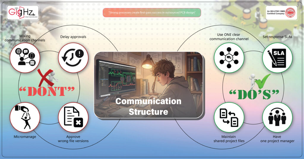
DO — What You MUST Do
- Use ONE clear communication channel
Pick one platform (Email / Slack / Teams).
All approvals + decisions should stay in that single thread, so no context is lost. - Set response SLAs
Vendor: reply within 12–24 hrs.
You: reply within 24–48 hrs.
This keeps both sides on schedule and prevents silent waiting periods. - Have one project manager
Only one person should communicate and approve schematic, layout, stack-up, etc.
This avoids confusion and conflicting instructions. - Do a short weekly sync
15–20 min call to review progress, blockers, and next milestones.
Short meetings prevent misunderstandings and keep momentum steady. - Maintain shared project files
One common folder with BOM, schematic PDFs, 3D, rules, snapshots, and review notes.
Everyone works with the same source of truth. - Use version-controlled file names
SCH_v1.0 → SCH_v1.1
Layout_v2.0
Clear versioning avoids confusion and prevents rework. - Clarify assumptions quickly
Vendor raises queries early.
You respond within 48 hrs.
Fast clarification prevents wrong routing decisions. - Keep a simple project dashboard
Status: Pending → In-Progress → Submitted → Approved.
A simple visible status prevents confusion about project state. - Document approvals
Write it in email/project system—never rely on memory. - Set escalation steps
If vendor delays → escalate to lead engineer.
If you delay approvals → vendor pauses safely.
DON’T — What You MUST Avoid
- Don’t mix communication channels
No Email + WhatsApp + Phone for the same project.
Mixing channels always leads to lost decisions. - Don’t delay approvals
Delayed feedback = delayed PCB.
Every day of silence pushes the schedule. - Don’t allow multiple internal people to message vendor
Causes conflicting instructions → redesign loops. - Don’t micromanage
No “update every hour.” Weekly sync + dashboard is enough. - Don’t send comments in scattered messages
Put all review notes in one place for clarity and traceability. - Don’t approve wrong file versions
Always check version history first. - Don’t hide changes
If mechanical/enclosure changes → inform immediately. - Don’t allow undocumented decisions
Every phone call must end with a written summary. - Don’t trust vendors who ask zero questions
Silence = assumptions = mistakes. - Don’t ignore early red flags
Poor communication in Week 1 → poor communication throughout.
2. Design Inputs and Documentation
DO
- Send the final schematic with correct net names and reference designators
- BOM with real manufacturer part numbers and footprint matched
- Board outline, connector placement, mechanical constraints clearly defined
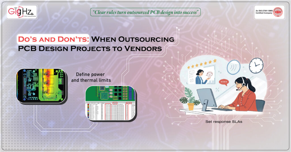
- Stack-up, target impedance, diff-pair rules in writing — not verbally
- Power and thermal limits defined (current, temperature rise)
- Include STEP or DXF mechanical files for clearance and enclosure alignment
- Provide readable PDFs + native design files so no assumptions are made
DON’T
- Don’t send “work-in-progress” schematic screenshots
- Don’t share BOMs without verified footprints
- Don’t leave impedance and length rules for vendor to guess
- Don’t delay sharing enclosure / mechanical updates
- Don’t assume the vendor knows your power budget or clearance rules
3. Timeline, Quality & Revision Control
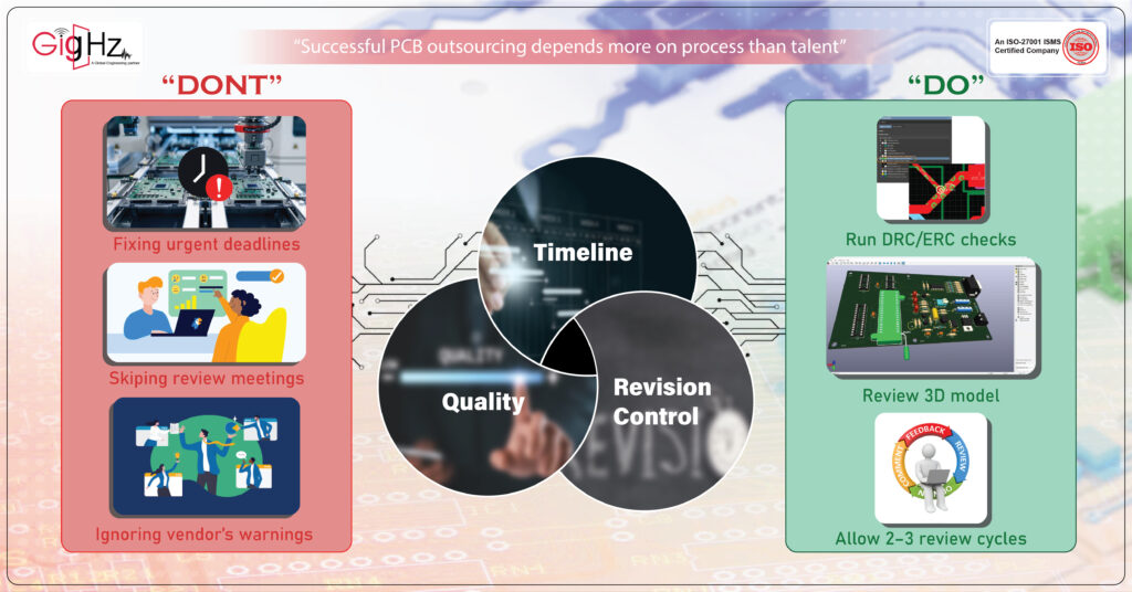
DO
- Freeze timeline: Schematic → Pre-layout review → Routing → Final review → Release
- Allow 2–3 review cycles, not unlimited iterations
- Use version tracking (v1.0 → v1.1 → v2.0) with change logs
- Run DRC/ERC checks before every review submission
- Review 3D model for collision, warpage, and connector fit before release
DON’T
- Don’t set unrealistic “urgent” deadlines
- Don’t skip review meetings to “save time” — it causes late-stage mistakes
- Don’t approve files without checking revision number
• Don’t ignore vendor’s warnings about manufacturability
4. NDA, IP Ownership & Export Files
DO
- Sign NDA before sharing any design data
- Confirm you own all design files, not just Gerbers
- Request complete export package at the end:
✔ Native CAD source files (.PrjPcb, .BRD, etc.)
✔ Gerber / ODB++
✔ Drill + stack-up reports
✔ Netlist + constraints
✔ STEP model - Final output must be delivered through E-mail with a download link + version number mentioned clearly.
This ensures legal proof of delivery and prevents confusion later.
- Define how long vendor must support post-handover issues (ex: 90 days)
DON’T
- Don’t work with vendors who refuse NDA
- Don’t accept only PDFs or screenshots as “final output”
- Don’t leave IP ownership undefined
- Don’t allow vendor to charge extra for source files later
Bottom Line
Outsourcing PCB design is not a shortcut.
It is a structured engineering partnership that must follow defined rules.
If you want first-pass success, you must:
✔ Communicate clearly
✔ Provide full design inputs
✔ Control timelines and revisions
✔ Protect your IP and output files
Do these right, and outsourcing becomes an advantage — not a risk.
Ignore them, and you face redesign loops, delays, and ownership headaches.
Clear rules protect your schedule, your budget, and your design.
Book a Call. Schedule a Free Consultation now. https://calendly.com/gighz/30min
Stuck in a loop of challenges? Always pick smart solution that works
Have you faced costly rework because 2D drawings skipped in MCAD workflows?
Effective way to prevent MCAD documentation errors recalls?
Please answer both poll questions before submitting.
Thank you for your response! 😊
Latest Post
Get Customized Engineering CAD Design Service

Book a Free Consultation Call
Partner with Gighz and bring your most innovative design concepts to life. Our engineering cad services accelerate development so you can focus on your big vision.