Why PDN Design Fails on Real PCB Despite Passing Simulation
- Posted On:
- October 26, 2025
- Category:
- Ecad
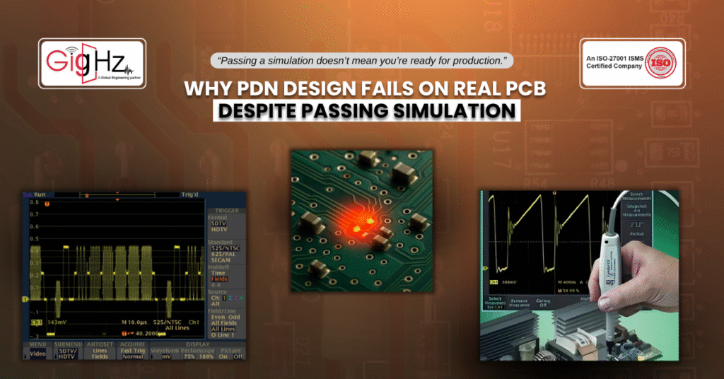
So, apparently, you must have run all the simulations, where everything looks stable, and the margins seem completely safe.
But when the board comes back from fabrication, the measurements don’t match the models.
This kind of PDN design failure after simulation is one of the most common and frustrating issues engineers face.
Now, on paper, the design is solid but in the lab, it went in a different direction.
So, what’s happening between simulation and real-world validation?
Let’s unpack it.
Why Simulations Don’t Always Match the Real PCB

So, when you compare PDN simulation vs real-world performance, the gap usually comes down to assumptions. Simulations work on idealized data, while real PCBs bring in parasitics, process variations, and environmental factors. That’s why PDN fails on real PCB even when the virtual model looks flawless.
Some of the most overlooked issues include:
- Incomplete stack-up data: If your material properties are assumed rather than measured, results shift.
- Missed package effects: Without including package inductance and resistance, you get optimistic results.
- Ignored high-frequency behavior: Also, Simulation tools may smooth over resonances that matter in practice.
Consequently, this is where the gap between simulation limitations in PDN analysis and lab measurements becomes clear—your tool isn’t wrong, but it isn’t modeling everything either.
Common Parasitics That Break PDN Designs
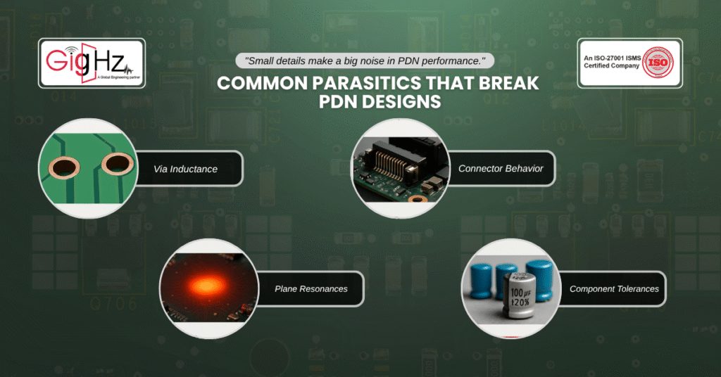
Every real PCB introduces details that models often skip! As, these PDN parasitics in real PCB builds can have dramatic effects:
- Via inductance at higher frequencies, vias behave very differently than assumed in flat simulations.
- Connector behavior where models rarely include the parasitics of connectors, sockets, and test points.
- Plane resonances at certain harmonics, copper planes turn into antennas rather than stable references.
- Component tolerances where a 20% tolerance capacitor can drastically change resonance points.
.
Therefore, Define target impedance (Z_target = ΔV/I) early — e.g., 50 mΩ for 1 A with ±50 mV ripple while ensuring PDN impedance stays below Z_target across frequency.
When these stack up, your board doesn’t behave like the simulated schematic anymore. Now, that’s why PDN fails on real PCB even if everything seemed fine during analysis.
Checklist: How to Close the Gap Between Simulation and Reality

If you want your design to survive the jump from simulation to hardware, you need to build checks around real-world PDN validation methods. Here’s a practical checklist:
- Validate your stack-up with the fab house and Don’t simulate assumed Dk/Df values to get the actual data.
- Model vias and connectors explicitly and use field solvers if needed, especially for high-frequency PDNs.
- Run corner simulations. Explore best-case and worst-case tolerances to capture manufacturing variability.
- Cross-check power with signal simulations! So, tie in decoupling strategies with simulation limitations in PDN analysis so that both domains align.
- Measure early! Do a pre-silicon lab validation of partial builds using real-world PDN validation methods before the full system is produced.
Therefore, by applying this checklist, you reduce surprises when the board comes off the
Real Example
An engineering team working on an automotive ECU passed every PDN simulation vs real-world performance test with flying colors. Yet, during hardware validation, the board repeatedly reset under high-speed PCIe transactions.
After investigation, the issue traced back to PDN parasitics in real PCB vias and planes that weren’t fully modeled. The simulation assumed perfect plane behavior, but in reality, resonances lined up with switching transients.
Now, they definitely passed all PDN simulations, showing impedance <30 mΩ. Yet during validation, the board reset under PCIe Gen3 traffic.
Also, Real measurements revealed a 120 mΩ spike at 180 MHz, matching a PCIe subharmonic. The issue came from unmodeled parasitics in vias and planes — the simulation assumed ideal behavior.
After adding 47 nF decaps and via stitching, impedance dropped 60%, and the resets stopped.
So, with that takeaway we realized that the simulations didn’t fail but the assumptions behind were not correct.
The Deeper Lesson from PDN Failures
Now, if you look at simulation limitations in PDN analysis, one fact stands out: no tool can perfectly capture reality on its own. That’s why you can’t stop at simulations—you need to verify.
Just as you’d never ship a DDR or PCIe design without compliance testing, you shouldn’t finalize a power design without real-world PDN validation methods. Simulation is the guide; measurement is the truth.
And that’s also why PDN fails on real PCB: So, basically it’s the difference between theoretical stability and practical reliability.
Bridging the Simulation-to-Reality Gap
Here are three steps that deliver quick improvements:
- Use better models and import vendor-provided S-parameters rather than generic values.
- Co-simulate and combine PDN and SI in one flow to spot interactions.
- Validate in stages! Yes, don’t wait until the full board and validate critical sections first using real-world PDN validation methods.
Likewise, these steps alone solve the majority of PDN simulation vs real-world performance mismatches.
Bottom Line
Summing, your PDN design doesn’t fail because simulation is useless—it fails because simulation is incomplete. So, to move beyond simulation limitations in PDN analysis, engineers must think in terms of both modeling accuracy and practical validation.
By accounting for PDN parasitics in real PCB designs and building in real-world PDN validation methods, you can close the gap and ensure your next design works as expected—both in software and in silicon.
Now, at Gighz, we integrate advanced modeling with lab validation to help teams catch why PDN fails on real PCB before it costs a spin.
Therefore, contact us today at info@gighz.net for a free consultation
Follow us at LinkedIn for more updates https://www.linkedin.com/company/3483128/admin/dashboard/
Stuck in a loop of challenges? Always pick smart solution that works
Have you faced costly rework because 2D drawings skipped in MCAD workflows?
Effective way to prevent MCAD documentation errors recalls?
Please answer both poll questions before submitting.
Thank you for your response! 😊
Latest Post
Get Customized Engineering CAD Design Service

Book a Free Consultation Call
Partner with Gighz and bring your most innovative design concepts to life. Our engineering cad services accelerate development so you can focus on your big vision.