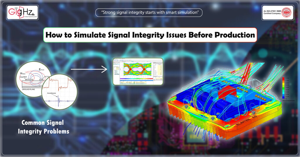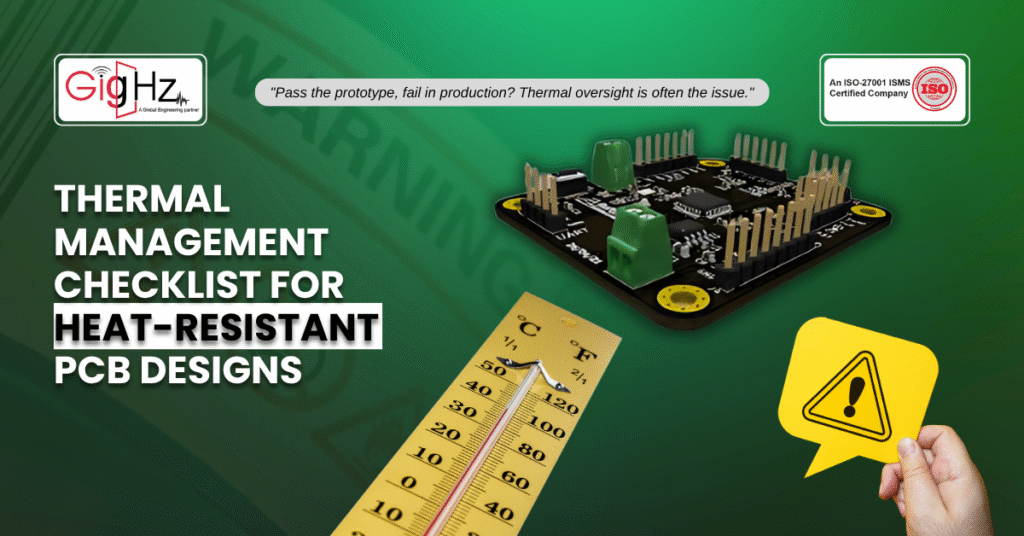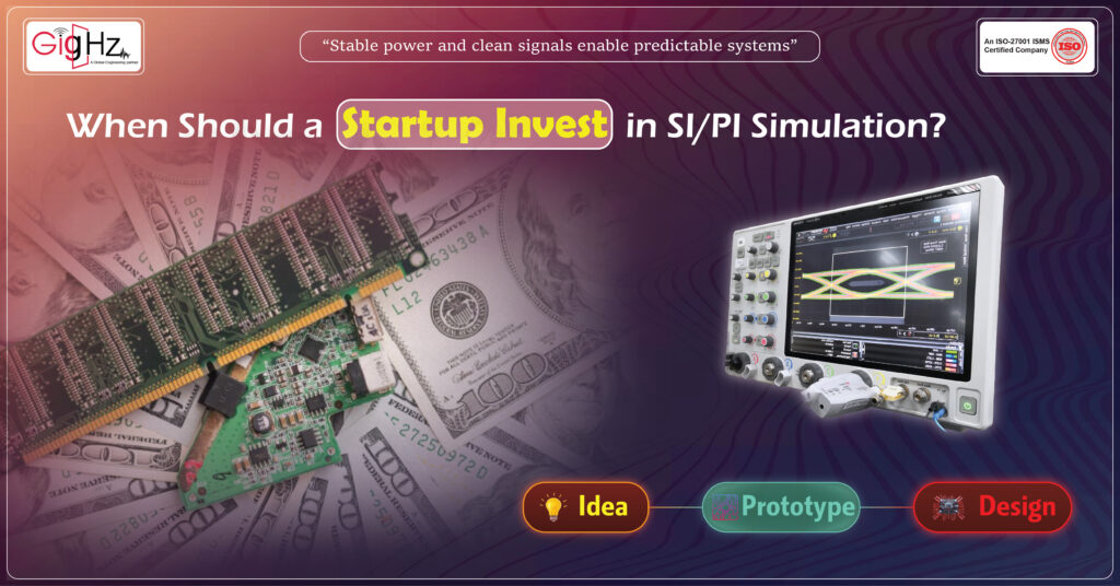
When Should a Startup Invest in SI PI Simulation?
Every hardware startup goes through the same emotional journey. The first prototype arrives. The LEDs blink. The firmware loads. The team feels a small moment of pride, as if they finally brought an idea to life. For a while, everything looks good. And then the board starts showing small cracks—random resets, unstable power rails, noisy
When Should a Startup Invest in SI PI Simulation? Read More »