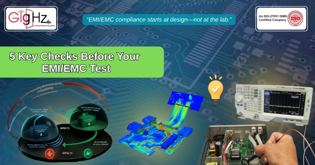
5 Essential Checks Before EMI/EMC Testing for Electronics
At times, getting your electronics item certified for EMI/EMC may feel like walking into a compliance inspection you think you’re ready for—until you fail. Likewise, EMI EMC analysis is not just about any last-minute tweaks before compliance testing. Rathter, It’s about integrating electromagnetic awareness right into your design process — even before your PCB even
5 Essential Checks Before EMI/EMC Testing for Electronics Read More »