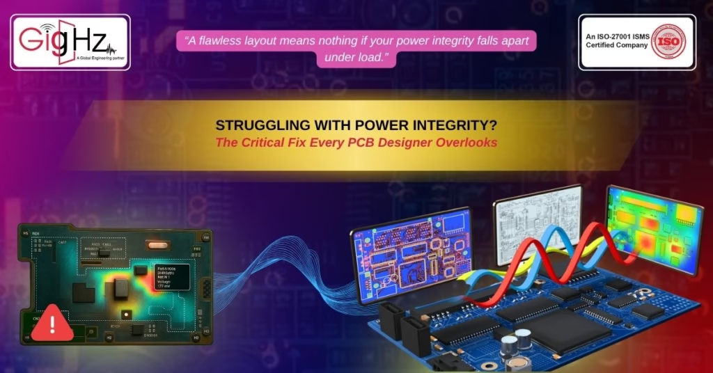
Struggling with Power Integrity? The Overlooked Fix Every PCB Designer Should Know
- Posted On:
- June 27, 2025
- Category:
- Analysis & Simulation
Now,
If you ever had a perfectly routed PCB that still failed in real-world performance tests, then chances are that the issue was not within your layout.
Probably, it was wrong with your pcb power integrity analysis.
Yes, in high-speed and high-density designs, even tiny oversights in power distribution leads to massive consequences like — unstable voltages, signal noise, or even lead to complete failure.
However, many engineers underestimate the importance of power integrity analysis in PCB design until it’s too late.
The Hidden Threat in Your Stack-Up
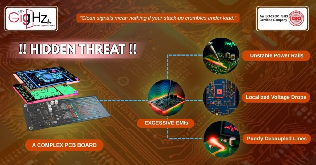
Nowadays, PCBs have dense multilayer designs, fine traces, and ICs with dynamic power demands. Even if simulations look clean, simultaneous current draw can stress the PDN and reveal hidden weaknesses.
Whereas, your signals might simulate just fine, but what happens when all those ICs draw current at once?
Likewise, without robust and efficient power integrity analysis tools, you may never spot:
- Localized voltage dips
- Unstable power rails
- Excessive ground bounces
- EMI from poorly decoupled lines
Plus, when these problems appear, it’s usually after the board gets manufactured.
How Power Integrity Issues Emerge and Undermine System Reliability
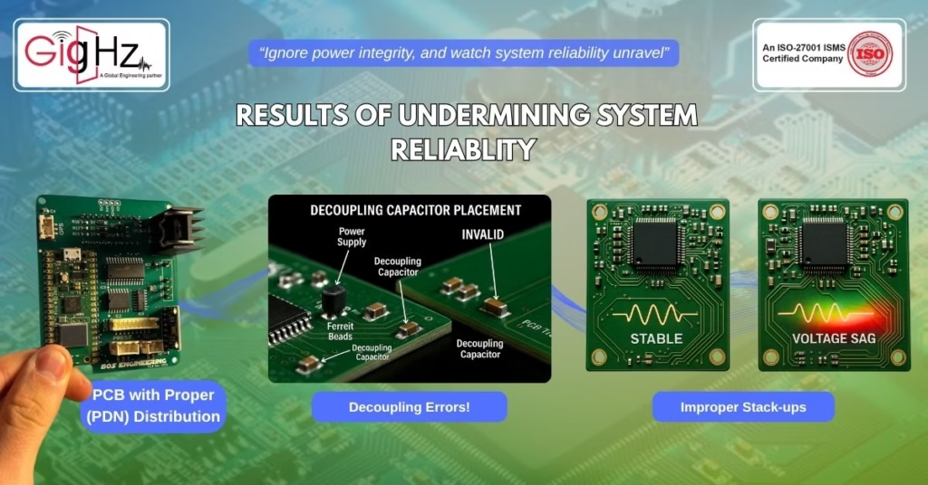
Primarily, most designs fail not because of flawed functionality, but because of overlooked basics in aspects of power management integrated circuit analysis and design.
Here’s what that looks like in practice:
- Your power delivery network (PDN) seems fine—until a high-speed processor pulls transient current, causing a voltage sag.
- Then, you’ve probably placed decoupling capacitors, but haven’t verified their resonance frequencies using power integrity analysis tools.
- Lastly, you assume your stack-up has enough plane area but haven’t simulated current density to check for hot spots.
So, each of these oversights compounds into erratic board behavior — and worse, those problems can masquerade as signal integrity or logic issues, leading you down the wrong debugging path.
A Real Fix Most Designers Overlook
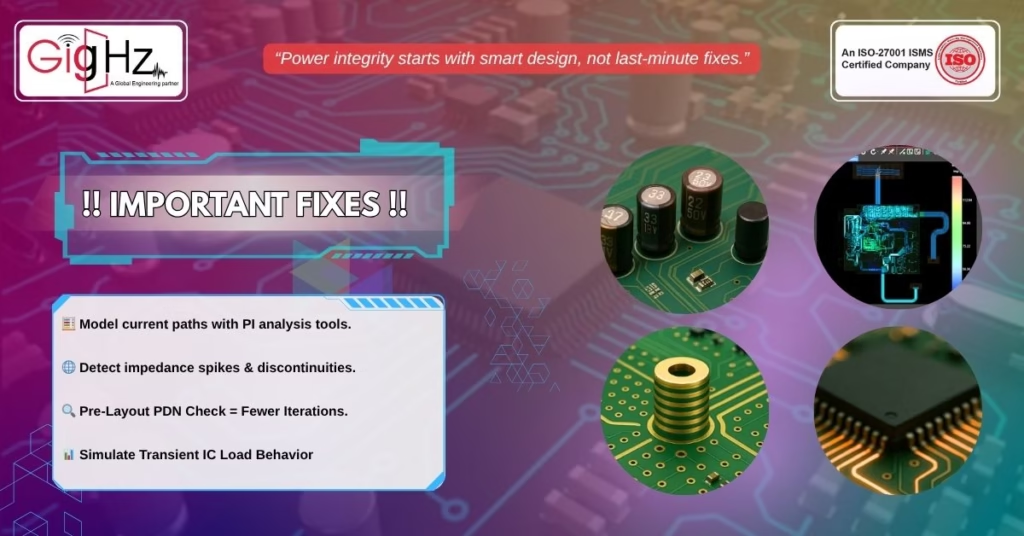
Now, here’s what top-performing teams do differently: Eventually, they simulate their PDN as early as possible.
Using specialized power integrity analysis tools, designers can model how current flows from power sources to each IC. Additionally, these tools also reveal how planes and vias interact and help identify locations where impedance discontinuities or spikes occur.
Besides, many of these insights can be gained before layout is even finalized. Moreover, it means that you can also design with clean power in mind, instead of firefighting after fabrication.
Quick Wins You Can Apply Today:
- Use decoupling capacitors with different ESR and ESL values: Don’t just use the same cap everywhere. Also, layer your values for wideband decoupling.
- Simulate the PDN early: Don’t wait until post-layout operations! Plus, pre-layout power integrity analysis in PCB helps make smarter design decisions.
- Optimize via placement for power planes: Also, the current doesn’t just flow magically. Likewise, it reduces path impedance with well-placed vias.
- Use stack-ups with controlled impedance and ample return paths: Poor plane design causes noise and ripple under load.
- Review every IC’s transient response: Good power management integrated circuit analysis and design looks at both steady-state and dynamic conditions.
Bottom Line
In summary, signal integrity issues are often immediately apparent, often underlying as distorted waveforms, data corruption, and elevated noise levels.
Therefore, power integrity analysis in PCB is not just optional anymore! Rather, it’s super critical. However, with the advent of modern power integrity analysis tools the process is more accessible and efficient than ever before.
Evidently, omitting power management IC (PMIC) analysis and design from your workflow significantly limits visibility into power distribution behaviors
Therefore, it’s highly recommended to consult experts beforehand! Feel free to Contact us at info@gighz.net
For more updates and enclosure design solutions follow us at- https://www.linkedin.com/in/chandra-thimma/
Latest Post
Get Customized Engineering CAD Design Service

Book a Free Consultation Call
Partner with Gighz and bring your most innovative design concepts to life. Our engineering cad services accelerate development so you can focus on your big vision.