Why Your PCB Fails EMI Compliance Even After Following the Rules
- Posted On:
- November 13, 2025
- Category:
- Analysis & Simulation
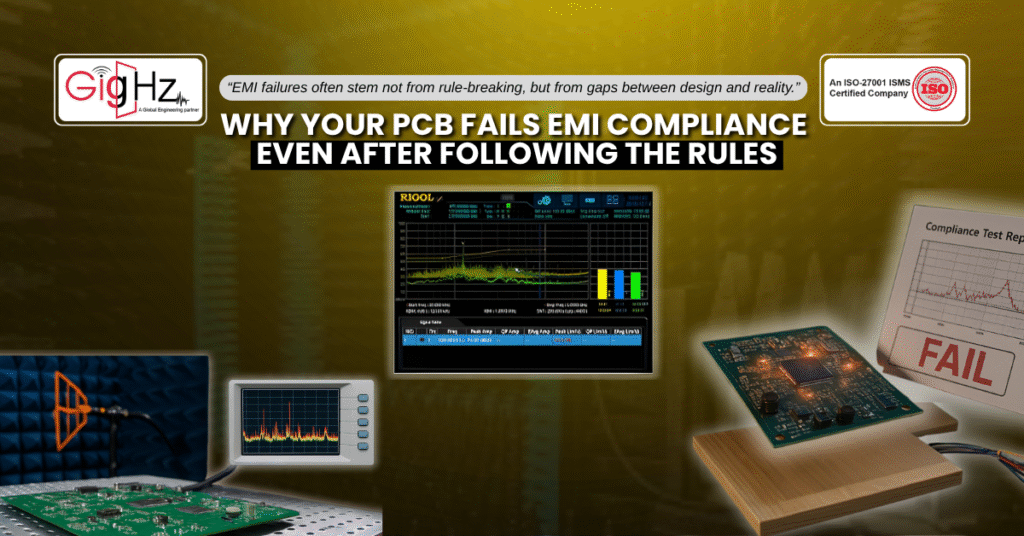
So, you must have followed every guideline in the book.
And, your stack-up looks correct, return paths seem clean, and your shielding strategy is by the standards.
Yet, during EMI compliance testing, the board fails.
Now, this is a scenario many engineers face — even when they’ve applied all the “right” practices for PCB design for EMI.
Now, the reality is that electromagnetic interference in PCBs isn’t always the result of ignoring standards.
Often, it comes from subtle design oversights, incomplete validation, or the difference between simulation assumptions and real-world environments.
Also, these gaps lead to failures in certification and trigger long cycles of PCB EMI compliance failure
In this post, let’s break down the common EMI design mistakes that slip through even disciplined workflows, and how to address them with practical steps.
1. Over-Reliance on Rule-Based DRC Checks
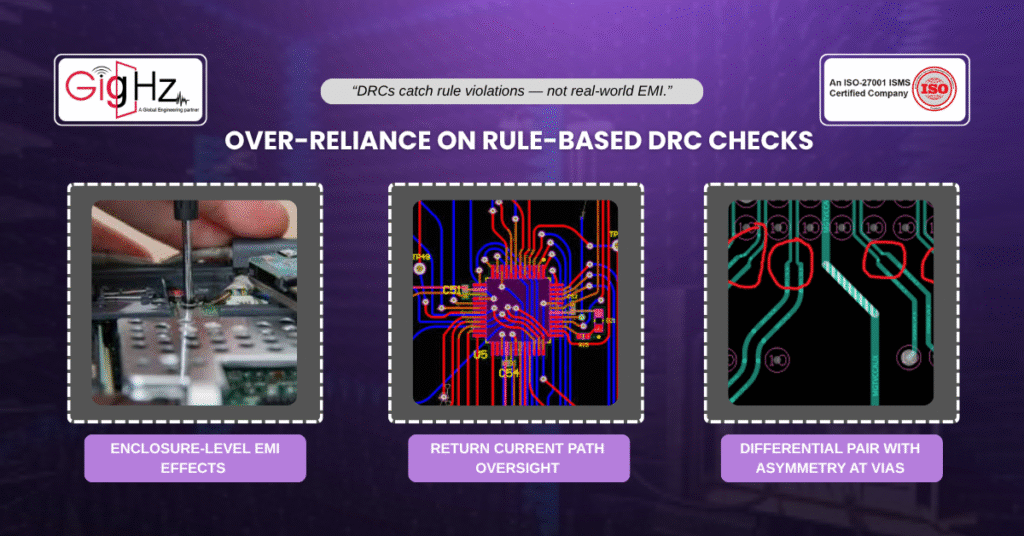
Now, most modern ECAD tools provide design rule checks (DRCs) with embedded EMI-related constraints.
While these are helpful, they aren’t sufficient. Now, passing a rule check does not guarantee PCB EMI compliance because rules are only as good as the constraints you set.
For example:
- DRC may flag trace width or spacing but won’t evaluate the quality of a return current path.
- It may confirm differential pair matching but won’t assess radiation from asymmetry at vias.
- It rarely considers enclosure-level effects that alter electromagnetic interference in PCBs during certification.
So, the fix?
Well, you must use DRCs as the first line of defense but supplement them with field solvers, EMI compliance testing prototypes, and manual layout reviews focused on real-world conditions.
2. Ground Planes Without Grounding Discipline
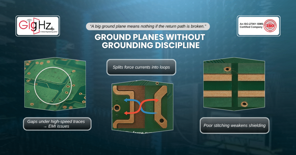
Also, many engineers believe that simply pouring a large ground plane ensures stability. But in PCB design for EMI, grounding strategy matters far more than sheer copper area.
Issues often arise from:
- Gaps in the return path, especially under high-speed traces.
- Splits in ground planes that force currents into unintended loops.
- Inconsistent stitching vias across layers that weaken shielding.
When EMI failure troubleshooting reveals unexpected peaks in emissions, poor return path management is often to blame. The corrective approach is to ensure continuous return paths, add stitching vias at transitions, and avoid unnecessary splits unless carefully engineered.
3. Layout That Looks Clean but Radiates in Practice
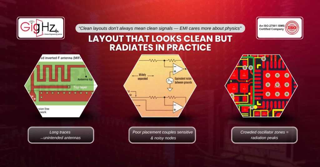
Now, even when a layout looks visually neat, it may not perform well under compliance testing. This is where the gap between theory and field validation becomes clear.
Key contributors include:
- Long trace lengths acting as unintended antennas.
- Poor component placement that forces sensitive nodes near noisy aggressors.
- Insufficient spacing around oscillators or clock generators, leading to radiation peaks.
So, applying layout tips to reduce EMI is about more than symmetry — Rather, it’s about minimizing coupling opportunities and ensuring critical nets have short, shielded paths.
Shielding and Filtering Misapplications
Additionally, adding shielding cans or filters often feels like an immediate fix, but misapplied techniques can worsen the problem. For example:
- A poorly grounded shield can increase radiation instead of containing it.
- Filter networks placed too far from the source lose effectiveness.
- Multiple ground connections without a clear reference create resonances.
As a result, it highlights that these scenarios highlight why common EMI design mistakes can persist even when standard mitigation elements are present. It’s not just what you add — it’s how and where you implement it.
Ignoring System-Level Interactions
Most importantly, a PCB doesn’t operate in isolation. Many EMI compliance testing failures happen because the system-level environment wasn’t considered. Power supplies, enclosures, and cabling all interact with the PCB’s electromagnetic profile.
For instance:
- A design may pass standalone validation but fail when mounted in a metal chassis due to resonance.
- Cabling harnesses can unintentionally couple noise and act as radiators.
- Heat sinks attached to switching devices can create new parasitic paths for emissions.
Now, that’s why the most reliable designs integrate PCB design for EMI with system-level EMC planning from the start.
Moving From Reactive to Preventive Design
The most important takeaway? Failing PCB EMI compliance is not about ignoring rules — it’s about relying only on rules without deeper validation. Passing DRCs and applying guidelines gets you part of the way, but the difference between passing and failing often comes down to:
- Recognizing the limits of ECAD automation.
- Building prototypes for early EMI failure troubleshooting.
- Treating electromagnetic interference in PCBs as both a board-level and system-level challenge.
Now, by embedding these practices into your workflow, you avoid chasing fixes late in the process and improve your chance of first-pass compliance.
Final Word
Summing up, every engineer wants their design to pass EMI compliance testing on the first attempt.
But the truth is, even well-structured designs can fail if subtle details are overlooked.
By going beyond DRC checks, refining grounding strategies, validating layouts under real-world stress, and considering system-level interactions, you significantly reduce the risk of surprises.
Likewise, at Gighz, we’ve helped teams refine their workflows, cutting down redesign cycles and improving pass rates in certification.
So, if you’re struggling with PCB design for EMI or need help with EMI failure troubleshooting, reach out at info@gighz.net — let’s make sure your next design clears compliance without delay.
Stuck in a loop of challenges? Always pick smart solution that works
Have you faced costly rework because 2D drawings skipped in MCAD workflows?
Effective way to prevent MCAD documentation errors recalls?
Please answer both poll questions before submitting.
Thank you for your response! 😊
Latest Post
Get Customized Engineering CAD Design Service

Book a Free Consultation Call
Partner with Gighz and bring your most innovative design concepts to life. Our engineering cad services accelerate development so you can focus on your big vision.