How to reduce the EMI and EMC in your PCB design Projects?
- GigHz
- January 29, 2025
- emi and emc
- Home
- Email Us

EMI and EMC
World of medical industry is constantly changing
One of the key players in this innovation is a printed circuit board.
Electromagnetic Interference (EMI) can significantly impact the functionality and accuracy of blood pressure monitors pcb.
Blood pressure monitors rely on Bluetooth or Wi-Fi to send real-time readings of blood pressure (e.g., systolic and diastolic values) to centralized systems.
However, these wireless signals can face interference from nearby electromagnetic sources.
Signal disruption could result in inaccurate or lost data, meaning real-time blood pressure readings may not reach healthcare providers as intended.
Interference might cause temporary connection drops, leading to delayed data transmission, especially critical in emergency care situations.
Once the blood pressure monitor collects data, it sends this information through the router to a cloud-based healthcare system.
Poorly shielded router hardware or network cables can also be susceptible to EMI.
If the router fails to properly receive data due to interference, blood pressure readings could be delayed or misprocessed, leading to incomplete patient records or failure to alert healthcare professionals in case of abnormal readings.
The data from the blood pressure monitor is often transmitted to a cloud platform for storage and analysis.
Wired or wireless paths between the router and the cloud-based servers could be compromised by external electromagnetic interference.
So, How to reduce the EMI and EMC in your PCB circuit design Projects?
Let’s dive into insights!
How to reduce the EMI and EMC in your PCB design Projects?

A low-inductance ground plane is essential in PCB design for reducing electromagnetic interference (EMI) and mitigating signal integrity issues.
A larger ground area on the PCB reduces the system’s ground inductance, which in turn helps decrease EMI emissions and crosstalk.
While there are various methods to connect signals to the ground, it’s important to understand what should not be done.
- Never connect PCB components randomly to ground points.
- Use a Full Ground Plane and Ground Grids
- Minimize Return Path Lengths
Faraday’s law dictates that the return current should follow the path of lowest impedance.
Impedance at any given frequency is described by the formula Z(w) = R + jωL.
At low frequencies, the impedance is primarily dominated by resistance (R), while at higher frequencies, the inductive component (jωL) becomes more significant.
This causes the return current to favor the path with the lowest loop inductance.
To optimize signal integrity, it is essential to:
- Keep return paths as short as possible.
- Minimize the loop area to reduce inductance.
- Ensure precise management of the return current paths.
Control Impedance
When designing high-speed circuits, it’s crucial to match the impedance between your signal source and destination.
If this impedance isn’t properly controlled, you can run into issues like signal reflection and high-frequency ringing, which can disrupt your signal integrity.
But the problems don’t stop there.
That excess RF energy from these reflections and ringing can bleed into other parts of your circuit, causing electromagnetic interference (EMI).
This is something you definitely want to avoid. So, how do you address this? The solution lies in signal termination.
By using signal termination techniques, you can reduce those unwanted reflections and ringing.
These methods help control the impedance and even slow down those fast-rising and falling signal edges, making your circuit run more smoothly.
Decouple Power and Ground
When ICs are running, they generate high-frequency switching currents that introduce noise into the power rails or traces connected to them. If this noise isn’t properly managed, it can lead to radiated emissions and EMI issues.
A key way to control power rail noise is by placing decoupling capacitors as close as possible to the IC’s power pins and grounding them directly to the ground plane. Using power planes instead of power traces also helps to minimize power noise and improve overall circuit stability.
Minimize Trace Lengths
Traces on a PCB serve as pathways that carry current from the driver to the receiver.
However, bends or intersections in these traces can create radiating antennas that interfere with signals. Here are some key trace design practices:
Trace Separation:
Maintain sufficient distance between signal traces (such as clock, video, audio, reset signals) by following the “3W rule”—spacing them at three times the width of each trace.
This minimizes crosstalk and coupling between traces on the same PCB layer, with differential traces as the exception. For more on reducing crosstalk, see our guide on HDI substrates.
Routing Differential Traces Closely:
Placing differential traces near each other enhances their coupling factor and maintains noise in common mode.
For instance, if two close traces pick up the same amount of external noise, it will affect both equally, allowing the noise to cancel out.
This is why high-speed signals are often routed as differential pairs.
Smart Use of Vias:
In multi-layer PCBs, vias enable signal routing between layers, but they also introduce capacitance and inductance.
Avoiding vias for critical traces when possible helps prevent impedance mismatches that can cause reflections.
When vias are necessary, add ground vias nearby to stabilize the characteristic impedance.
For differential pairs, ensure an equal number of vias in each trace, and consider using a shared anti-pad to reduce parasitic capacitance.
Avoiding Stubs on Sensitive Traces:
Stubs on high-frequency traces create reflections and can act as unwanted antennas.
Minimizing stubs is crucial for maintaining signal integrity on sensitive traces.
Add Shielding
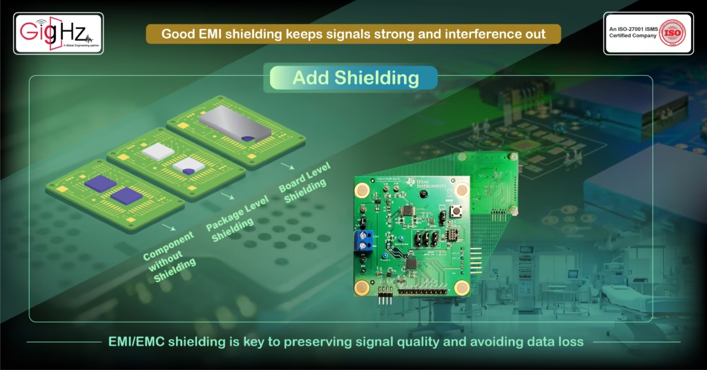
Shielding is all about keeping your signals clean and interference-free.
By using conductive or magnetic materials—or both—we can effectively cut down on electromagnetic interference (EMI) in your system.
Picture a grounded, closed-off container that acts as a protective shield, absorbing and reflecting radiation to keep unwanted noise out.
Whether you need to shield the whole system or just specific parts, EMI/EMC shielding is key to preserving signal quality and avoiding data loss.
For instance, cables carrying analog or digital signals are well known for causing EMI issues due to their built-in capacitance and inductance.
A simple fix?
Shield the cables and ground them at both ends, which drastically cuts down on interference and ensures your signals stay strong and clear.
PCB layer stack-up
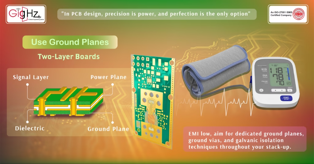
When it comes to reducing electromagnetic interference (EMI) in your PCB, the way you arrange your layers can make a world of difference.
If your board has two or more layers, try to dedicate one layer as a ground plane. This provides a solid reference point and reduces interference.
For a four-layer board, here’s an ideal setup: layer one is for signals, followed by a ground layer, then a power layer, and finally, another signal layer.
This stack-up not only keeps your PCB efficient but also helps control impedance, especially if you route high-speed signals on the top layer.
- Using Two-Layer Boards? If a full ground plane isn’t feasible, create a grid structure for grounding to maintain stability.
- No Separate Power Plane? Make sure to run ground traces parallel to power traces to keep your supply as clean as possible.
- Working with More than Four Layers? Try alternating between signal and ground/power layers, and stick to an even number of layers. This pattern gives you a solid grounding structure and helps reduce interference between layers.
To keep EMI low, aim for dedicated ground planes, ground vias, and galvanic isolation techniques throughout your stack-up.
Isolate Sensitive Components to Reduce Interference
Here’s a rule of thumb: group components on your PCB based on the signals they work with—analog, digital, power, low-speed, high-speed, etc. This approach creates “zones” on your PCB, minimizing interference. Try to keep each signal group within its zone. And when signals do need to cross from one group to another, consider adding a filter to ensure a smooth, interference-free transition.
Summary
In the realm of pcb design, adhering to effective design guidelines is crucial for ensuring electromagnetic compatibility (EMC).
A well-structured pcb layout can significantly reduce EMI (electromagnetic interference), which is essential for good EMC performance in any electronic device.
One should address the source of EMI during the design process to prevent potential emc problems that could arise from poorly designed pcb layouts or insufficient pcb stackup considerations.
Latest Post
Get Customized Engineering CAD Design Service

Book a Free Consultation Call
Partner with Gighz and bring your most innovative design concepts to life. Our engineering cad services accelerate development so you can focus on your big vision.