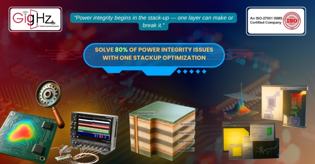
How One PCB Stackup Change Can Fix 80% of Power Integrity Issues
- Posted On:
- June 23, 2025
- Category:
- Analysis & Simulation
Now, here’s something that most engineers don’t realize until it’s way too late!
Yes, I am talking about power Integrity analysis which isn’t just about the power rails or decoupling caps.
Accordingly, it often goes much deeper inside the PCB board’s stack-up itself.
Truly, you might be doing everything “by the book” till, like placing your capacitors right, keeping return paths short.
However, you still run into serious performance issues at times.
Now, that’s probably because of improper layer arrangement!
Consequently, your entire power integrity analysis and management for integrated circuits practices can collapse anytime.
When Power Delivery Looks Right, But Isn’t!
As we all know that contemporary PCBs have transformed into more complex and multilayer structures.
Likewise, it is characterized by high-speed signal transmission, high component density, and significant power delivery requirements.
Why do even clean designs face certain issues of instability?
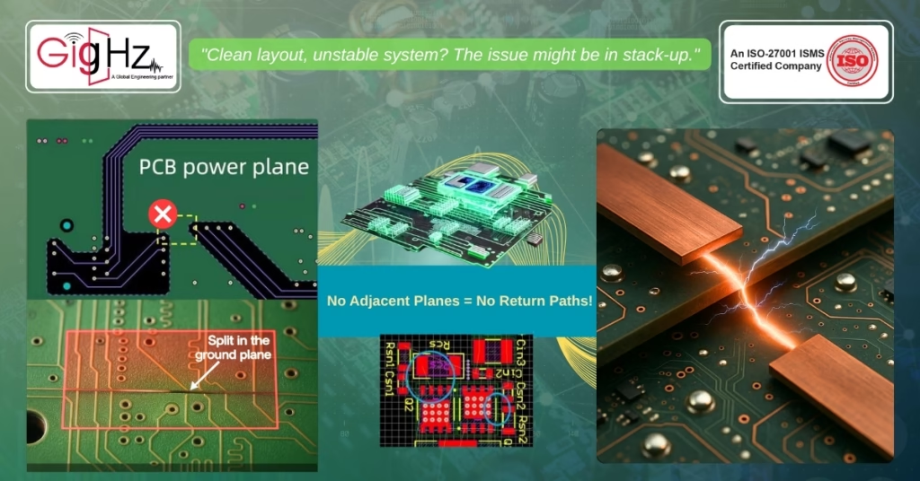
Now, that’s because the power integrity analysis in PCB often overlooks the physical structure of the board. Yes, if your power and ground planes are not adjacent or don’t form a solid return path – Then, no amount of simulations or patchwork fixes can help you!
Therefore, the problem may not be in your layout — rather, it may be your stack-up.
How Bad Stackups Ruin Perfect Designs

Now, allow me to walk you through some real-world scenarios.
As, we were working on a high-speed ECU board for an automotive system, using the best power integrity analysis tools available. Consequently, our pre-layout simulations looked great. Likewise, we followed all the best practices for decoupling and even optimized trace widths accordingly.
But once we built the prototype, it escalated into some following critical issues like:
- Random resets
- Voltage dips under transient load
- And of course, massive EMI problems
So, it turned out that power and ground layers were separated by two signal layers. Due to that one oversight it created a high loop inductance path, which made all our decaps useless.
On the other hand, the stack-up was not supporting any clean return paths and that broke down everything.
Now, this isn’t a rare scenario! We have seen it over and over, especially in designs where power management integrated circuit analysis and design wasn’t considered alongside board construction.
One Stack-Up Fix That Changes Everything
Now, after correcting the layer sequence and putting the power and ground planes right next to each other — we immediately saw the stability improve drastically.
Evidently, this one crucial modification reduced the noise, stabilized the core voltage, and brought our EMI levels within speculations. Also, the power integrity analysis in PCB confirmed that the ripple and overshoot were immensely reduced.
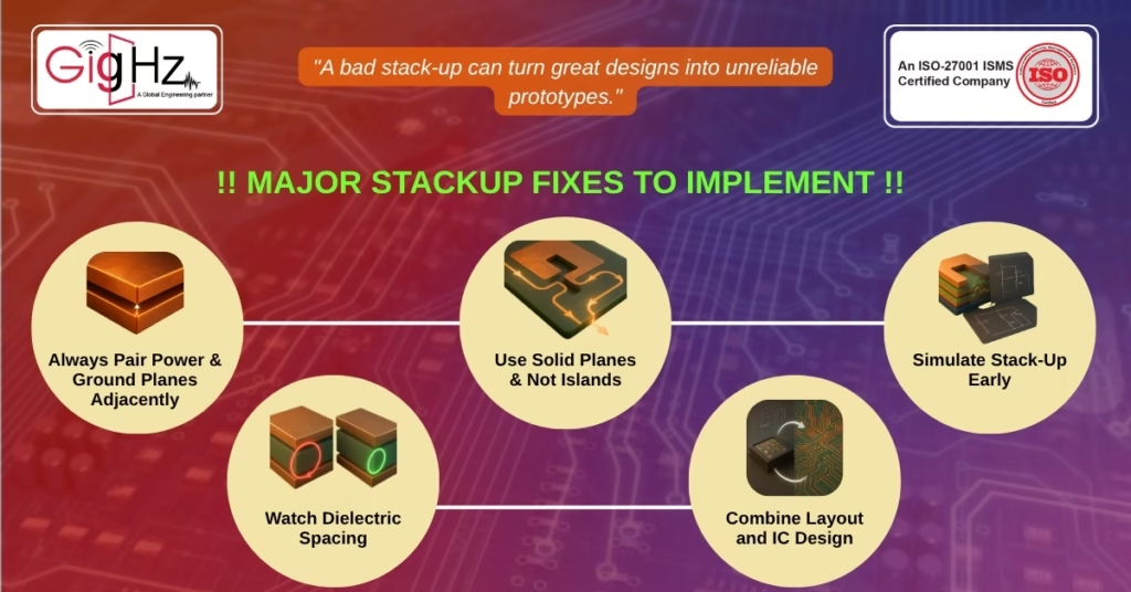
So, here’s the following checklist as a best-practice guide for everyone to follow:
- Always Pair Power and Ground: Put them on adjacent layers for tight return paths.
- Use Solid Planes, Not Islands: Breaks or gaps in planes cause return current detours and introduce noise.
- Simulate Stack-Up Early: Accordingly, use power integrity analysis tools that factor in your physical layout, not just circuit schematics.
- Watch Dielectric Spacing: Yes, thinner dielectrics = lower loop inductance.
- Combine Layout and IC Design Thinking: Yes, make sure that power management integrated circuit analysis and design is done in syncing with board designing. Otherwise, your IC will behave differently in theory than on the board itself.
Apparently, we have applied this to over 30 projects in the past few years. In nearly all of them, the stack-up was a hidden bottleneck extensively. But, once optimized for power integrity analysis and management it showed better margins, lower ripple, and fewer errors.
Bottom Line
Summing up, most engineers over-focuses on components and pay secondary attention to the construction. However, if your power integrity analysis in PCB is not backed by the right stack-up, then it won’t matter how good your tools are at all.
Therefore, always prioritize the layer stack-up to efficiently handle signal integrity, power delivery, and thermal management.
Need a hand in analyzing yours? Likewise, we use advanced power integrity analysis tools tailored for real-world PCB environments and not any textbook assumptions.
Contact us at info@gighz.net and avail a free consultation call today.
Latest Post
Get Customized Engineering CAD Design Service

Book a Free Consultation Call
Partner with Gighz and bring your most innovative design concepts to life. Our engineering cad services accelerate development so you can focus on your big vision.