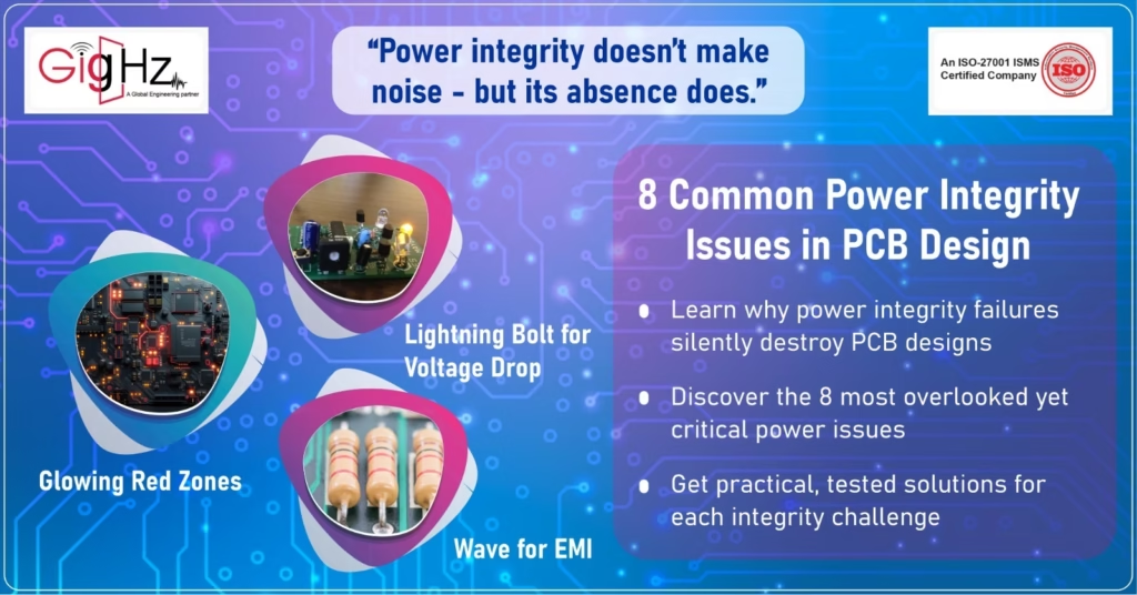
8 Common Power Integrity Issues in PCB Design (and How to Solve Them)
- Posted On:
- May 7, 2025
- Category:
- Analysis & Simulation
Your PCB design will face silent destruction due to power integrity issues! And, they will strike even before you realize something is wrong. Your months of PCB layout refinement work can be ruined by a basic power delivery mistake, which you did not spot until your design fails under operating conditions. Engineers experience this nightmare often because they fail to understand power integrity which silently determines the success or failure of their complete design.
The backbone of every high-performance circuit is power integrity and considering it just a basic technical checklist will be a mistake. The failure of power integrity results in processors freezing up while signals become distorted and thermal runaway causes component destruction. Things can get even worse. The problems typically appear during prototyping or during compliance testing or end up being discovered by customers who receive the products.
Modern electronics systems demand the maximum capacity from their power delivery systems. The combination of quick edge rates with minimal voltages and strict noise margins creates absolutely no tolerance for mistakes. A processor operating at high speed can experience a complete failure when power drops by just 50mV. When capacitors receive incorrect placement they transform ground planes into antennas. Your circuitry will gradually cook itself through inadequate thermal design. But, there’s good news. You can prevent these errors, if you know where to inspect.
This guide will reveal the 8 most damaging power integrity issues in PCB design and time tested solutions to prevent them from destroying your PCB.
1. Power rail collapse- voltage levels drop resulting in performance drop
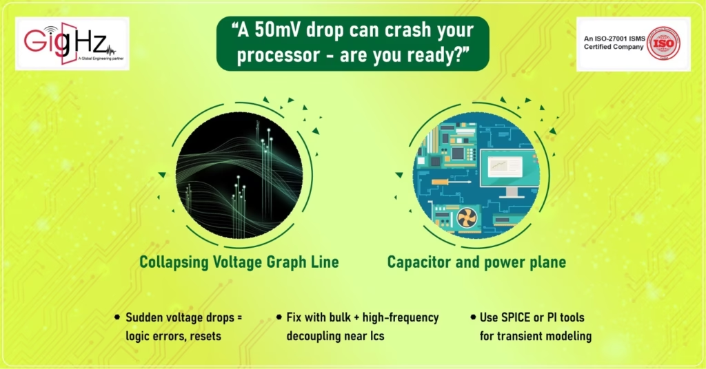
The voltage supplied to an IC experiences power rail collapse, when it descends beneath its operational threshold because of either high PDN impedance or excessive current demand. High-speed digital circuits are affected most by sudden current spikes from CPU state changes because these events create temporary voltage drops that trigger logic errors or resets.
How to Solve It
Power rail collapse becomes avoidable through the reduction of PDN impedance levels. Low-resistance power planes serve as better high-current paths than thin traces do. The placement of bulk capacitors near power sources together with localized high-frequency decoupling capacitors near ICs provides stable voltage during transient loads.
The analysis tools such as SPICE or dedicated power integrity analyzers enable modeling of transient responses to help detect PDN weaknesses before production. You should either increase copper thickness or add multiple power paths in parallel to minimize resistance issues.
Ground Bounce Operates as an Under-the-Radar Signal Killer
Multiple ICs switching states at the same time produces ground bounce effects because of parasitic inductance, which results in temporary voltage spikes in the ground reference. The noise generates errors that trigger false circuit activation and jitter in high-speed interfaces.
How to Solve It
The successful reduction of loop inductance represents the solution for ground bounce elimination. This means:
- IC power pins should have ground vias positioned as near as possible to minimize return path length.
- The use of multiple decoupling capacitors creates low-impedance high-frequency current paths.
- A solid ground plane should replace daisy-chained grounding because the technique increases inductance.
The use of differential signaling provides benefits in high-speed applications because it eliminates ground noise. The early design phase benefits from power integrity simulations which help identify ground bounce effects so designers can optimize their placement strategies for components and decoupling methods.
3. Insufficient Decoupling: The Hidden Cause of Noise
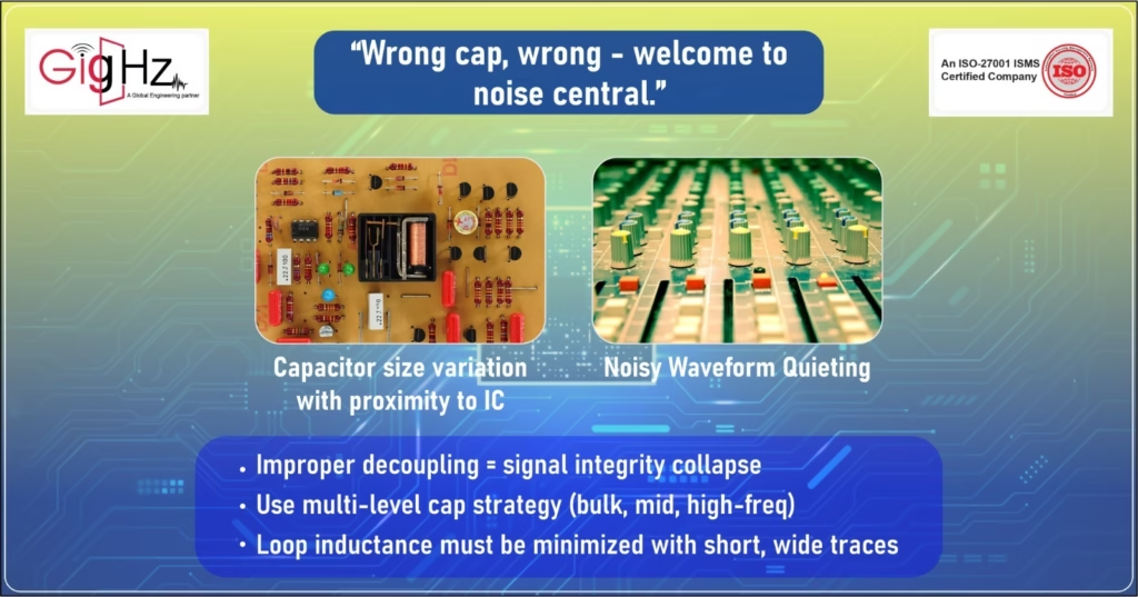
The purpose of decoupling capacitors is to function as local power storage units that deliver immediate current to ICs. Decoupling capacitors lose their power noise and signal integrity functionality, when either incorrectly selected or located too distant from power pins.
How to Solve It
A successful decoupling strategy needs multiple steps to achieve its goals.
- Keep power pins within a few millimeters distance from each capacitor placement.
- The frequency response benefits from using three capacitor types: bulk (10-100µF), mid-range (0.1-1µF) and high-frequency (1-100nF).
- You should reduce loop inductance through wide and short traces with multiple vias that lead from capacitors to power and ground planes.
Simulation tools enable users to find the best capacitor configurations that meet their particular PDN impedance requirements.
4. The destructive effects of power loss due to excessive heat generation
PCB traces and components that experience high current flow produce heat that can result in thermal stress or solder joint failures or component burnout, when left unmanaged. Power electronics, motor drivers, and high-performance computing require special attention to this factor.
How to Solve It
The first step of thermal management depends on designing PCBs intelligently.
- For high-current paths use wider traces combined with thicker copper material that is at least 2oz.
- The placement of thermal vias beneath hot components will direct heat into the inner ground planes.
- The placement of heat-sensitive elements should be at a distance from high-power devices according to good component placement practices.
The thermal simulation software Ansys Icepak and SolidWorks Flow Simulation enables hotspot predictions which helps users optimize copper pours and implement heatsinks or airflow enhancements before production.
5. Impedance Mismatch in Power Delivery Networks
An impedance mismatch within the PDN generates reflections, which produces voltage ripple and noise. The tight requirements of high-speed edge rates make impedance control essential for avoiding problems in these designs.
How to Solve It
To maintain consistent impedance:
- The design should implement continuous power and ground planes, while avoiding any breaks under high-speed signal routes.
- The use of each via creates inductance, which disrupts impedance performance.
- Run simulations to check PDN impedance performance across all frequencies for compliance with established specifications.
The frequency-domain impedance analysis can be conducted using tools like HyperLynx and Cadence Sigrity. It enables users to optimize decoupling networks and plane shapes.
6. Poor Grounding: The Root of Many Noise Problems
The integrity of a ground system determines loop inductance, which results in noise coupling, electromagnetic interference, and signal integrity problems. Two main errors in design practice involve improper star grounding of mixed-signal circuits and incorrect partitioning of ground planes.
How to Solve It
- Design your ground plane without splits unless split planes are required for isolation purposes.
- The separation of analog and digital grounds at one point will stop ground loops from forming in mixed-signal designs.
- Multiple ground layer vias should be used for stitching to minimize impedance.
To verify EMI/EMC compliance and noise immunity, designers should simulate the ground system design.
7. Inadequate Component Placement: A Layout Nightmare
The positioning of components improperly generates unwanted resistance, inductance, and thermal problems. For example- if high-speed processors are located distant from their decoupling capacitors, it can result in power integrity failures.
How to Solve It
- Keep related components together (decoupling caps should be placed next to IC power pins).
- The distance between power and ground paths should remain short to minimize areas with high current flow.
- The layout of switching regulators should follow manufacturer guidelines.
You should use 3D EM simulation software to evaluate current distribution patterns and enhance layout optimization in the design phase.
8. Insufficient Design for Manufacturability (DFM)
When simulation results match production needs, but actual production yields different results then poor DFM practices are usually to blame. Issues with inadequate copper balancing or wrong via design, or unattainable trace tolerances result in power integrity problems, when boards are manufactured.
How to Solve It
- Use IPC standards to determine trace width along with spacing measurements and via dimensions.
- Equal distribution of copper across the board must be maintained to stop warping when undergoing reflow.
- Your PCB manufacturer should help you validate design rules before you finalize the layout.
Altium Designer and Mentor Xpedition tools include DFM checks that enable users to identify potential manufacturing problems ahead of time.
Conclusion: Proactive Power Integrity = Reliable PCBs
Power integrity requires initial correct design because it cannot be solved with post-production solutions. The eight critical issues of power rail collapse, ground bounce, decoupling, heat, impedance, grounding, placement, and DFM enable you to prevent noise and voltage drops, and thermal failures.
You should use simulation tools along with smart layout practices and seek manufacturer collaboration to build strong PCB designs. Designs that undego power integrity analysis tools benefit from both: failure prevention and enhanced performance results that satisfy compliance tests and demonstrate long-term reliability. Your ability to excel in power integrity will make your designs stand out against competitors in both high-speed digital boards and precision analog circuits.
The mastery of power integrity leads to failure prevention and design reliability which results in market domination, especially in the current electronics industry.
CTA- Book a consultation call
So next time when you plan a PCB layout, ask yourself an importance question-Is the power delivery network secure and dynamic, as it should be? If not, then connect with us.
For more updates on PCB designs and resolving power integrity issues you can follow us at- https://www.linkedin.com/in/chandra-thimma/
Outbound links-
https://www.ecadstar.com/en/blog/power-integrity-in-pcb-design/
https://resources.pcb.cadence.com/blog/2020-the-basics-of-power-integrity-in-pcb-design
Latest Post
Get Customized Engineering CAD Design Service

Book a Free Consultation Call
Partner with Gighz and bring your most innovative design concepts to life. Our engineering cad services accelerate development so you can focus on your big vision.