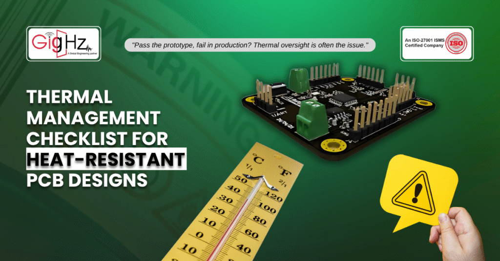
Thermal Management Checklist for Heat-Resistant PCB Designs
- Posted On:
- November 6, 2025
- Category:
- Analysis & Simulation
So, are you sure that your boards handle the heat?
Yes, It’s a question that every PCB designer faces, because thermal issues don’t just reduce performance!
Apparently, they also shorten the lifespan, cause intermittent failures, and in worst cases, result in expensive redesigning.
In fact, many prototypes pass initial electrical validation only to fail under load because thermal management wasn’t prioritized early.
That’s why having a thermal management checklist for PCB design is essential if you want to avoid surprises and build reliable electronics.
So, whether you’re working on automotive systems, industrial controls, or consumer devices, following PCB thermal design best practices will save you from late-stage failures and keep your projects on schedule.
Likewise, down below we have a simple framework that you can apply, blending thermal analysis for PCBs with layout and documentation practices to help you prevent PCB overheating in real-world conditions.
1. Start with Placement and Power Density Awareness

Now, component placement is not about only fitting everything within the outline! It’s where thermal success or failure begins. Evidently, grouping multiple high-power devices together creates local “hot spots” that even the best heatsinks or thermal vias and PCB cooling solutions struggle to fix.
Key checks for placement discipline:
- Distribute high-power devices evenly to avoid concentrated heating zones.
- Keep heat-sensitive parts like sensors and oscillators away from regulators or MOSFETs.
- Ensure airflow paths exist between high-dissipation components.
Following these PCB temperature management techniques at this stage saves hours of debugging later.
2. Design Heat Paths into Your Layout
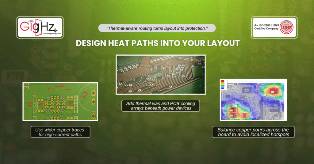
es, routing is more than signal integrity, it’s also heat integrity. Likewise, in terms of PCB thermal design best practices recommend embedding heat flow into your copper planes and traces.
Practical steps for thermal-friendly layouts:
- Use wider copper traces for high-current paths to reduce resistive heating.
- Add thermal vias and PCB cooling arrays beneath power devices to transfer heat into ground planes.
- Balance copper pours across the board to avoid localized hotspots.
These simple design tweaks turn the board into a passive heatsink, helping you prevent PCB overheating under load.
3. Validate with Simulation Before You Build

Now, even when layouts look thermally sound, it’s risky to rely on assumptions. So, running thermal analysis for PCBs before tape-out gives you a data-driven view of risk.
Checklist for simulation-driven validation:
- Run airflow and load condition scenarios in your CAD tool.
- Compare predicted junction temperatures against safe operating limits.
- Apply PCB temperature management techniques like thicker copper or added vias if hotspots appear.
. - Run steady-state and transient thermal sims using tools like Icepak, FloTHERM, or Cadence Celsius.
- Track θJA and θJC to ensure thermal reliability and avoid overheating issues.
Also, simulation saves money by preventing re-spins and ensures your design is heat-ready before it ever hits fabrication.
Beyond the Checklist: Why Documentation Matters
Now, thermal thinking doesn’t stop at the layout tool!
Subsequently, any boards failed not because the designer ignored heat, but because the assembler didn’t know the thermal intent.
Clearly documenting requirements — from stack-up details and copper thickness to heatsink mounting instructions — ensures manufacturing partners understand the design as intended.
Without it, the risk of gaps in execution rises, and your carefully designed PCB thermal design best practices may never make it into production.
Now, to close that gap, collaboration between design and manufacturing teams is key.
Therefore, thermal simulations, design notes, and even annotated diagrams should accompany the final files.
This bridges intent with implementation.
Include assembly drawings that show airflow direction and keep-out zones for heat-sinks or fans.
Without this, there’s a real risk that your carefully engineered thermal design never makes it into production as intended.
So, to close that gap, tight collaboration between design and manufacturing teams is essential.
Case Study
A telecom board initially ran 20°C above its thermal specification due to clustered power regulators creating hotspots. To address this, the team:
- Redistributed the placement of power regulators to improve heat spreading.
- Added 24 thermal vias per regulator pad to enhance heat dissipation through the PCB layers.
As a result, hotspot temperatures dropped by 18°C, allowing the board to pass stress validation without requiring a full redesign. This approach saved both time and cost while ensuring reliable thermal performance.
Bringing It All Together
Clearly, managing heat in electronics isn’t about last-minute fixes — it’s about designing with foresight.
By starting with smart placement, embedding thermal vias and PCB cooling strategies into routing, and validating with thermal analysis for PCBs, you create designs that stand up to real-world stress.
When you combine these with clear documentation and consistent use of PCB temperature management techniques, you don’t just prevent PCB overheating — Also, you build a system that’s reliable, scalable, and cost-effective.
By starting with smart placement, embedding thermal vias and PCB cooling strategies into routing, and validating with thermal analysis for PCBs, you create designs that stand up to real-world stress.
So, when you combine these with clear documentation and consistent use of PCB temperature management techniques, you don’t just prevent PCB overheating — also, you build a system that’s reliable, scalable, and cost-effective.
Key thermal design best practices include:
- Component Placement: Keep high-power components away from heat-sensitive ones and ensure good airflow paths.
- Thermal Vias: Use arrays of thermal vias under hot components to conduct heat to inner or opposite layers.
- Copper Pour Optimization: Maximize copper areas for heat spreading and reduce thermal resistance.
- Heatsinks & Thermal Pads: Finally, select and mount heatsinks properly, and use thermal interface materials where needed.
Final Word
Every engineer faces the same choice: design for thermal stability now or fight heat issues later. The checklist above gives you a practical framework rooted in PCB thermal design best practices that reduces risk and boosts reliability.
At Gighz, we’ve helped teams move from constant overheating issues to consistent first-pass success by embedding thermal thinking into their process.
Therefore, contact us today at https://calendly.com/gighz/30min for a free consultation.
Let’s make sure your boards not only power up but stay cool under pressure.
Stuck in a loop of challenges? Always pick smart solution that works
Have you faced costly rework because 2D drawings skipped in MCAD workflows?
Effective way to prevent MCAD documentation errors recalls?
Please answer both poll questions before submitting.
Thank you for your response! 😊
Latest Post
Get Customized Engineering CAD Design Service

Book a Free Consultation Call
Partner with Gighz and bring your most innovative design concepts to life. Our engineering cad services accelerate development so you can focus on your big vision.