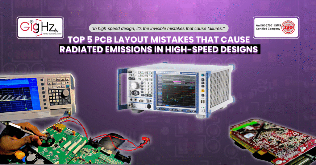
Top 5 PCB Layout Mistakes That Cause Radiated Emissions in High-Speed Designs
- Posted On:
- November 6, 2025
- Category:
- Ecad
So, you must have optimised the schematic, chosen the right components, and even double-checked stack-up rules.
But when the board hits EMI testing, it fails.
Now, this is often the result of subtle PCB layout mistakes causing radiated emissions—issues that don’t show up in design reviews but quickly surface in the compliance lab.
In high-speed designs, even a tiny oversight can trigger test failures.
Let’s break down the top five high-speed PCB EMC design errors that create radiated emission problems—and how to avoid them.
1. Ignoring Return Paths
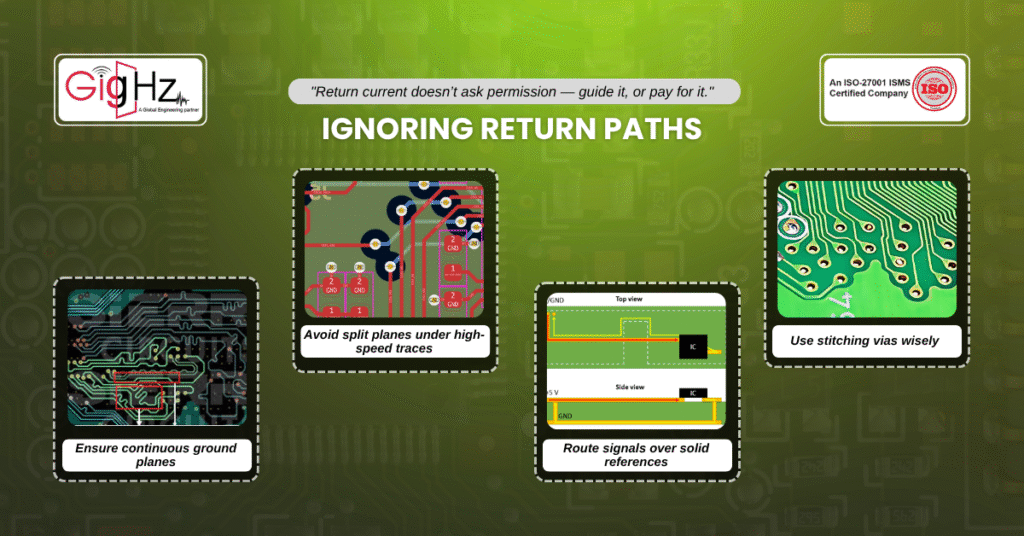
Now, one of the most frequent high-speed PCB EMC design errors is neglecting return current flow. So, signals always find a way back to their source, and if you don’t provide a clean, low-inductance path, they’ll couple into unwanted areas.
To prevent this, follow these best practices:
- Ensure continuous ground planes: A solid, uninterrupted ground plane allows return currents to follow tightly under the signal trace, minimizing loop area.
- Avoid split planes under high-speed traces: Splits force return currents to detour, increasing loop size and EMI.
- Route signals over solid references: Whether it’s a ground or power plane, always give your signal a stable, low-impedance return path.
- Use stitching vias wisely: Place them near layer transitions to maintain return current continuity in multi-layer designs.
A poor return path in high-speed layout creates large current loops, which act like antennas radiating noise. Consequently, this not only drives up emissions but also risks signal integrity.
Likewise, this is one of the simplest yet most powerful layout tips to reduce EMI — and a foundational principle of clean, reliable high-speed design.
2. Placing Decoupling Capacitors Incorrectly
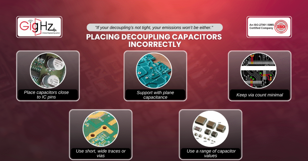
Decoupling capacitors are meant to suppress noise, but placement matters. If they’re too far from the IC pins or connected with long vias, they lose effectiveness.
Now, this error falls under classic high-speed PCB EMC design errors because it creates resonances that amplify emissions. When power delivery becomes unstable, it complicates high-speed PCB EMI troubleshooting and forces costly re-spins.
So, apply these placement best practices:
- Place decoupling capacitors as close as possible to the IC’s power pins — ideally on the same layer to reduce inductance.
- Use short, wide traces or vias to minimize loop inductance between the cap and the IC.
- Support with proper plane capacitance and combine discrete capacitors with low-inductance power/ground planes for broadband noise suppression.
- Use a range of capacitor values to mix small (e.g., 0.01 µF) and larger (e.g., 1 µF) caps to cover different frequency ranges effectively.
- Keep via count minimal between cap and IC also each via adds inductance — the fewer, the better.
3. Overlooking Differential Pair Balance
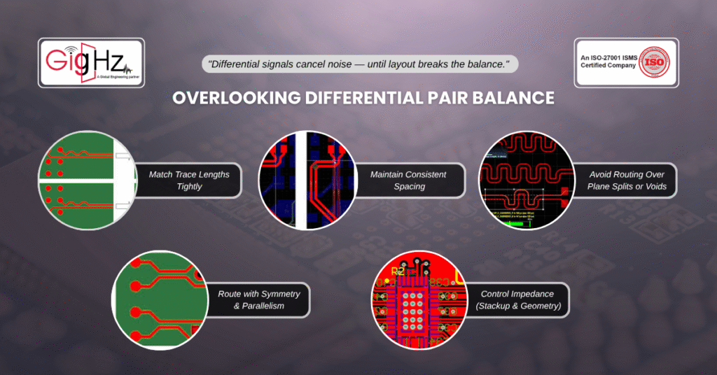
Differential signals are powerful tools for reducing EMI — but only if routed with precision. Any imbalance in trace length, spacing, or reference plane continuity causes these signals to radiate rather than cancel out, defeating the purpose of differential routing.
Consequently, this is a frequent PCB layout mistake, especially in high-speed interfaces like PCIe, USB, SATA, or DDR, where even minor skew can create radiated emissions and degrade signal integrity.
To maintain proper differential performance and reduce EMI:
- Match trace lengths tightly and even small mismatches (e.g., 50 mils) can cause timing skew and common-mode noise.
- Maintain consistent spacing between the pair as sudden spacing changes create impedance discontinuities and reflections.
- Avoid routing over plane splits or voids — reference plane discontinuities introduce imbalance and mode conversion.
- Route with symmetry and parallelism and especially through bends, vias, and connector transitions.
- Control impedance using stackup and trace geometry and target differential impedance (e.g., 90Ω for USB, 100Ω for PCIe).
Most importantly, maintain symmetry in routing, tightly control impedance, and avoid abrupt transitions. Also, these layout tips are essential to reducing EMI and ensuring signal integrity in high-speed differential designs.
.
4. Poor Layer Stack-Up Choices
If reference planes are spaced too far from signal layers (more than ~10 mils), impedance control becomes difficult and EMI rises. A poorly designed stack-up increases loop inductance and reduces shielding effectiveness.
Likewise, the best practices are to:
- Use tight coupling between signal layers and their reference planes to control impedance accurately.
- Design symmetric stack-ups to minimize warpage and crosstalk.
- Place critical high-speed signals adjacent to solid reference planes for low EMI and better signal integrity.
5. Long Stubs & Uncontrolled Vias
Now, via stubs longer than ~200 mils create resonances above ~3 GHz, which can severely degrade signals in PCIe, USB, DDR, and other high-speed interfaces. Uncontrolled vias also add unwanted inductance and impedance discontinuities.
- Use back-drilling or via-in-pad techniques to minimize or eliminate via stubs.
- Limit the number and length of vias in high-speed signal paths.
- Plan via placement carefully to maintain consistent impedance and reduce reflections.
Why These Mistakes Keep Happening
Finally, the truth is, many engineers know these rules! Also, the challenge is balancing speed, cost, and functionality under real-world deadlines. Under pressure, it’s easy to let layout tips to reduce EMI slip or underestimate the impact of a poor return path in high-speed layout.
But compliance testing doesn’t care about schedules—every design must meet standards. And when boards fail, it’s often traced back to these same five high-speed PCB EMC design errors.
But compliance tests such as CISPR 32 Class B or FCC Part 15 Sub B don’t forgive layout oversights—even a 3 dB spike can fail certification. As compliance doesn’t care about schedules, and when boards fail, it’s often traced back to these same five high-speed PCB EMC design errors.
Checklist: Avoiding EMI Failures in High-Speed Designs
Here’s a quick checklist to keep on hand during your next layout review:
- Verify continuous ground return paths for every high-speed signal.
- Place decoupling capacitors as close as possible to IC power pins.
- Maintain differential pair balance (length, spacing, impedance).
- Choose stack-ups that tightly couple signals to ground.
- Shorten and terminate high-speed traces properly.
- Use proper termination resistors (e.g., 85Ω for PCIe, 100Ω for USB) to prevent reflections in differential pairs.
- Minimize via count in high-speed signal paths — ideally fewer than 2 vias per trace to reduce discontinuities and signal loss.
As a result, this checklist doesn’t replace full EMC simulations, but it helps prevent the most common PCB layout mistakes causing radiated emissions before you reach the lab.
Now, on a 10-layer PCIe Gen4 board, emissions exceeded CISPR limits by 6 dB at 400 MHz—but by tightening decoupling placement and removing via stubs, the issue was resolved without a re-spin.
Final Word
Summing up, most issues stem from a handful of recurring design oversights. Likewise, by mastering layout tips to reduce EMI and applying disciplined reviews, you’ll catch errors before they show up in testing.
And if you do run into emissions trouble, structured high-speed PCB EMI troubleshooting—starting with return paths, stack-up checks, and decoupling strategy—often resolves issues faster than trial and error.
Therefore, preventing poor return paths in high-speed layout and other high-speed mistakes isn’t just about passing compliance.
At Gighz, we help teams spot and fix high-speed PCB EMC design errors early with proven design reviews and simulation support.
Therefore, contact us today at https://calendly.com/gighz/30min for a free consultation.
Stuck in a loop of challenges? Always pick smart solution that works
Have you faced costly rework because 2D drawings skipped in MCAD workflows?
Effective way to prevent MCAD documentation errors recalls?
Please answer both poll questions before submitting.
Thank you for your response! 😊
Latest Post
Get Customized Engineering CAD Design Service

Book a Free Consultation Call
Partner with Gighz and bring your most innovative design concepts to life. Our engineering cad services accelerate development so you can focus on your big vision.