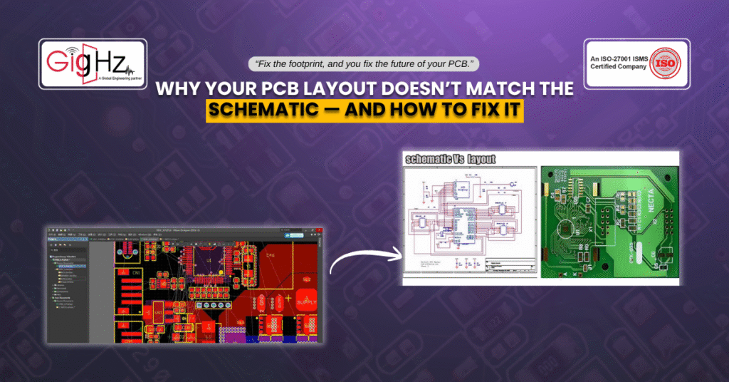
Why Your PCB Layout Doesn’t Match the Schematic — and How to Fix It
- Posted On:
- October 17, 2025
- Category:
- Ecad
So, you have double-checked your design, right?
Likewise, the schematic is clean, ERC passed, and you are feeling confident. But when you push the design to layout, the problem hits significant:
As a result nothing fits.
Now, this dreaded PCB layout doesn’t match schematic problem and it’s apparently more common than you think.
Engineers worldwide lose days (sometimes weeks) chasing mismatches between schematic symbols and footprints.
Consequently, this issue usually boils down to one thing: footprint mismatch in PCB layout.
So, whether it’s a swapped pin, wrong pad size, or flipped orientation, the issue develops ripple effects that stall projects, waste prototypes, and inflate costs.
But here’s the good news that you can fix it!
And better yet, you can prevent it from ever happening again.
Why Layout Mismatches Happen
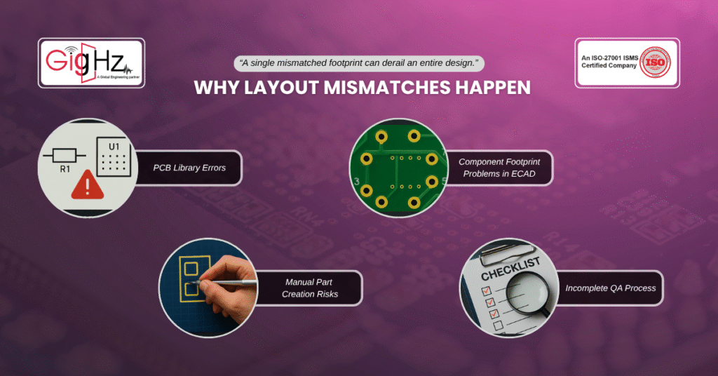
So, before we dive into how to fix layout mismatches, let’s understand the root causes in the first place. As most problems come from library and process gaps, not from schematic design itself. Now, here are the usual suspects:
- PCB Library Errors – A symbol that looks perfect in the schematic but points to an outdated or incorrect footprint.
- Component Footprint Problems in ECAD – Pads sized incorrectly for the package, missing courtyard data, or pin numbers not mapped correctly.
- Manual Part Creation Risks – When engineers create custom footprints in a rush without following IPC standards.
- Incomplete QA Process – No second eyes on the part library before releasing it into the design.
And the result?
Well, the schematic calls for one thing, but the PCB tool interprets it completely differently.
A Real Example: When Nothing Fit
We once worked with a client designing an industrial controller.
Everything looked great until they hit the layout.
Likewise, the connectors didn’t align, the regulator package didn’t match the manufacturer’s datasheet, and two ICs had swapped pin numbers.
What was the cause of it?
A series of PCB library errors compounded by inconsistent naming conventions.
By the time they noticed, a week of layout effort was wasted—and prototype costs doubled.
Consequently, this experience taught us) an important lesson that fixing footprint mismatch in PCB layout after the fact is expensive.
Therefore, preventing it is far cheaper.
How to Fix Layout Mismatches
So, If you’re already facing the issue, here’s a structured approach:
1. Audit the Library Immediately
Start by checking the components causing error and then compare the ECAD footprint against the manufacturer’s datasheet. Look closely at:
- Pin numbers and orientation marks
- Padstack dimensions
- Courtyard and keep-out areas
Likewise, this is the fastest way to identify component footprint problems in ECAD.
2. Trace the Mapping
Ensure the schematic symbol’s pin mapping matches the footprint’s pin assignment. Often, what looks like a random mismatch is simply a misaligned pin map.
3. Correct the Master Library
Don’t just fix the component in your project. Update the master library so the error doesn’t repeat in future designs. This also helps keep team members aligned.
4. Validate with Automation
Also, use built-in tool checks (like “package verification” or DRC extensions) that compare symbol-to-footprint mappings. Many ECAD platforms can flag these errors early if the settings are enabled.
5. Apply a QA Checklist
Adopt a standard PCB design review checklist that includes symbol-to-footprint verification. This ensures issues are caught before layout even begins.
Preventing Future Problems

While fixing errors is necessary, prevention is where you’ll save the most time and money. Now, here’s how to bulletproof your workflow:
- Centralize Your Library – Stop storing parts in local project folders. Use a managed library system so all designers pull from the same verified source.
- Enforce Standards – Adopt IPC-compliant naming and footprint creation rules.
- Run Footprint Verification Early – Add a step in your design flow to check footprints right after symbol creation.
- Peer Reviews – Even in small teams, a second engineer should review any newly created footprint before it goes live.
- Document Learnings – If a PCB library error happens, record the fix and add it to a shared guide for the team.
Quick Checklist: How to Fix Layout Mismatches Fast

So, here’s a condensed version you can apply today:
- Identify mismatched parts in layout.
- Cross-check footprints with datasheets.
- Validate pin mapping symbol-to-footprint.
- Correct and lock changes in the master library.
- Run automated ECAD checks.
- Re-spin layout with verified parts.
Hence, following this process consistently reduces costly re-spins and keeps schedules intact.
Bottom Line
Summing up, the issue of footprint mismatch in PCB layout doesn’t waste your resources and time — But, it undermines confidence in your whole design process. Likewise, every error costs time, money, and reputation.
But the fix isn’t rocket science: strengthen your library, enforce standards, and bake verification into your process. So, that’s how you avoid endless rounds of schematic says one thing whereas layout does another.
Similarly, At Gighz, we’ve helped clients recover from critical PCB library errors and implement bulletproof workflows that stop mismatches before they happen.
Therefore, always validate your libraries beforehand, consider engineering with consistent standards. Finally, execute with confidence knowing your schematic and layout will always align.
Contact us at info@gighz.net for a free consultation.
Stuck in a loop of challenges? Always pick smart solution that works
Have you faced costly rework because 2D drawings skipped in MCAD workflows?
Effective way to prevent MCAD documentation errors recalls?
Please answer both poll questions before submitting.
Thank you for your response! 😊
Latest Post
Get Customized Engineering CAD Design Service

Book a Free Consultation Call
Partner with Gighz and bring your most innovative design concepts to life. Our engineering cad services accelerate development so you can focus on your big vision.