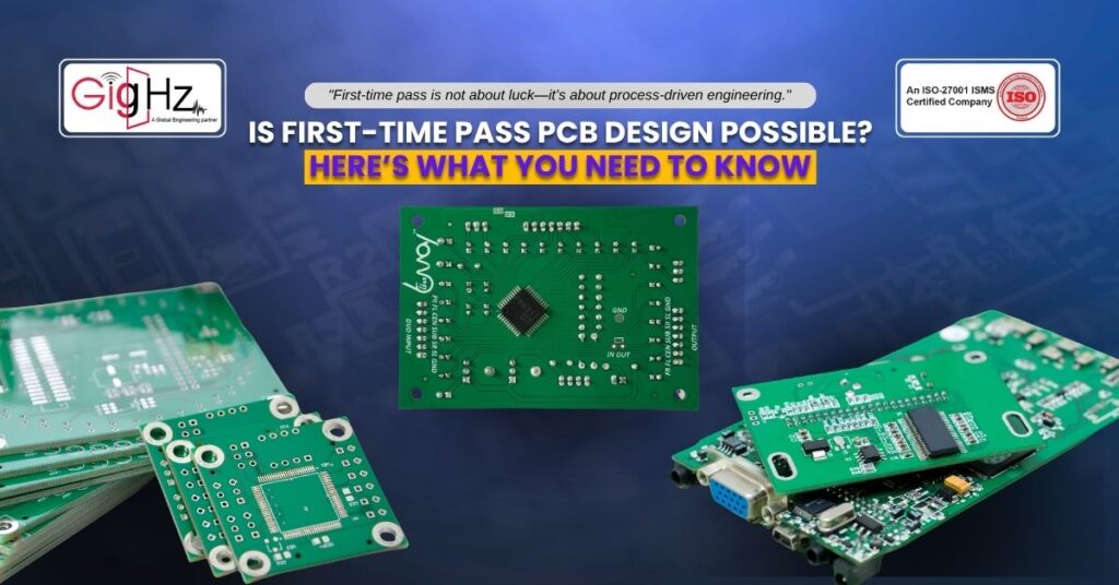
Is First-Time Pass PCB Design Possible? Here’s What You Need to Know
- Posted On:
- October 8, 2025
- Category:
- Ecad
Truly, every engineer dreams of having a First-Time Pass PCB Design process!
Accordingly, sending a board for fabrication, then getting it assembled, and seeing it work flawlessly on the first go.
Moreover, No re-spins, no unexpected failures and of course no budget overruns. But is that even realistic, or just wishful thinking?
Well, the truth is, while “zero re-spin” might sound a bit far-fetched, it’s actually possible when you know what pitfalls to avoid.
Also, how to build discipline into your design process.
Most failed first passes come down to avoidable errors, and with the tool usage.
Plus, other validation approaches, your design has a strong shot at first-pass yield.
Behind Failed First Passes
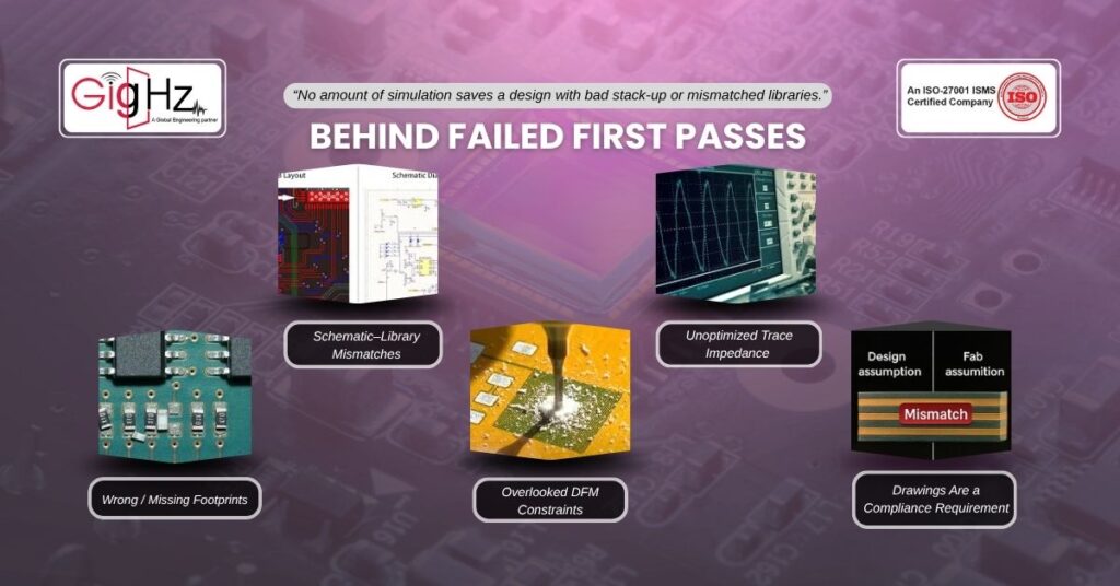
So, in our work with automotive and industrial boards, we see the same common PCB design mistakes come up again and again. Also, these are not some random problems! Evidently, they’re often the basics that slip through under deadline pressure:
- Missing or incorrect footprints that create assembly issues
- Unclear net connections due to schematic-library mismatches
- Overlooked DFM constraints like drill-to-copper clearances
- Unoptimized trace impedance in PCB leading to signal integrity issues
- Inconsistent stack-up assumptions between design and fab vendor
Apparently, none of these are exotic problems, but each one can kill a first-pass build. On the other hand, when you are scaling to production these mistakes multiply into schedule delays and wasted dollars.
Why Tools Alone Won’t Save You
Now, modern ECAD tools for error-free PCB design come with plenty of automated checks—DRC, ERC, constraint managers, and even 3D previews. But here’s the catch:
- It can only flag what you tell them to check.
Also, if your design rules don’t match your fabricator’s real-world process, or if your constraints aren’t fully defined, Also, you will still get green lights while hidden risks lurk beneath the surface.
Besides, the tool is only as strong as the engineer who configures it.
That’s why first-pass success is as much about process requirements as it is about technology.
First Pass Yield: Why It Matters
So, some teams assume that two or three re-spins are just “the cost of doing business.”
But let’s run the math here.
A single re-spin for a 6-layer automotive control board can cost:
- $8K–$15K in fab and assembly
- 4–6 weeks of schedule slip
- Hours of debugging and root-cause analysis
Likewise, multiply that across multiple projects, and the lost engineering bandwidth alone is crushing itself.
Now, this is why first pass yield in PCB design is not just a “nice-to-have metric.”
It directly impacts competitiveness, launch timelines, and profitability.
The Three Pillars of First-Pass Success
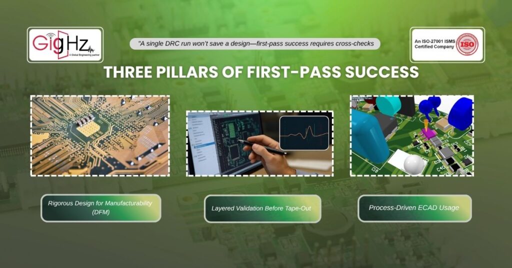
Evidently, from our experience, achieving high first-pass yield requires a balanced focus across three dimensions:
1. Rigorous Design for Manufacturability
Now, applying design for manufacturability PCB practices upfront prevents surprises later. So, that means:
- Validating minimum trace/space against your fab’s actual capability
- Checking via aspect ratios and drill tolerances
- Avoiding exotic finishes unless absolutely required
- Confirming assembly clearances and solderability early
2. Layered Validation Before Tape-Out
Also, relying on a single ERC or DRC run isn’t enough. Besides, practical PCB design validation tips include:
- Cross-checking schematics against BOM and netlists
- Reviewing stack-up impedance profiles with the fabricator
- Running signal integrity checks on high-speed nets
- Performing a manual visual “red pen” review, not just tool automation
3. Process-Driven ECAD Usage
Above all, the best engineers treat their ECAD tools for error-free PCB design like safety nets, not crutches. So, that means:
- Defining rulesets that match real-world fab and assembly capabilities
- Validating footprints in 3D and ensuring model-to-part consistency
Quick Checklist: Boosting Your First-Pass Success

Now, here’s a practical starting point for your next project:
- Validate every footprint against the datasheet
- Align stack-up assumptions with your fab vendor before routing
- Define real-world clearance and impedance rules in your ECAD tool
- Perform a peer review with another engineer, not just tool checks
- Simulate high-speed nets and power integrity risks before tape-out
So, follow these steps consistently, and you’ll already be miles ahead of the other teams.
Bottom Line
Summing up, is first-Time Pass PCB Design possible?
Yes!
Absolutely but only if you stop treating it like luck and start treating it like a process.
Likewise, by avoiding common PCB design mistakes, leveraging ECAD tools for error-free PCB design properly, and applying robust PCB design validation tips. Plus, you can dramatically improve first pass yield in PCB projects.
Also, add design for manufacturability PCB checks into the mix, and your chances of success climb even higher.
Because in the end, first-pass success isn’t about perfection but about discipline and ethics.
Similarly, at Gighz we have helped teams across industries to move from two or three costly re-spins per project to hitting >90% first-pass yield.
So, If your team is tired of delays and hidden mistakes, it’s time to rethink your process.
Validate smarter and implement precise engineering for manufacturability!
Also, execute with discipline and prevent re-spins before they happen.
Contact us at info@gighz.net to get a free consultation.
Stuck in a loop of challenges? Always pick smart solution that works
Have you faced costly rework because 2D drawings skipped in MCAD workflows?
Effective way to prevent MCAD documentation errors recalls?
Please answer both poll questions before submitting.
Thank you for your response! 😊
Latest Post
Get Customized Engineering CAD Design Service

Book a Free Consultation Call
Partner with Gighz and bring your most innovative design concepts to life. Our engineering cad services accelerate development so you can focus on your big vision.