How to Avoid Crosstalk at 16GHz in High-Speed Automotive PCB Design
- Posted On:
- September 29, 2025
- Category:
- Ecad
Undoubtedly, at 16 GHz, even the tiniest layout oversight can turn into a full-blown performance disaster.
That’s why we learned this the hard way on a recent EV controller project, where crosstalk in PCB design almost derailed our timing margins completely.
That too…just a few days before prototype release.
Likewise, in high-speed automotive boards, crosstalk doesn’t just mean “a bit of noise.”
Apparently, it’s skewed eye diagrams, failed compliance tests, and unpredictable behavior under thermal stress.
Also, the higher your frequency you get the more unforgiving the board becomes.
But here’s the good news! Clearly, you can stop crosstalk before it starts—with the right combination of signal integrity tips for 16GHz boards.
In addition with high-speed PCB layout tricks, and proven PCB crosstalk mitigation methods.
The 16 GHz Problem: Why Crosstalk Hits Harder
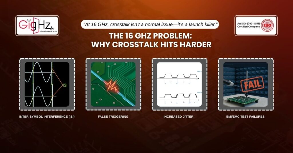
Now, at lower speeds, minor coupling between traces might pass unnoticed. But at 16 GHz, capacitive and inductive coupling can cause extensive:
- Inter-symbol interference (ISI) that limits maximum data rate
- False triggering on sensitive differential pairs
- Increased jitter, impacting timing closure
- EMI/EMC test failures, delaying certification
Moreover, the worst part? Also, these issues don’t always show up in basic functional testing—they reveal themselves at the worst possible moment often during system integration or compliance testing.
The Case Study: Saving a Launch with Pre-Layout Mitigation
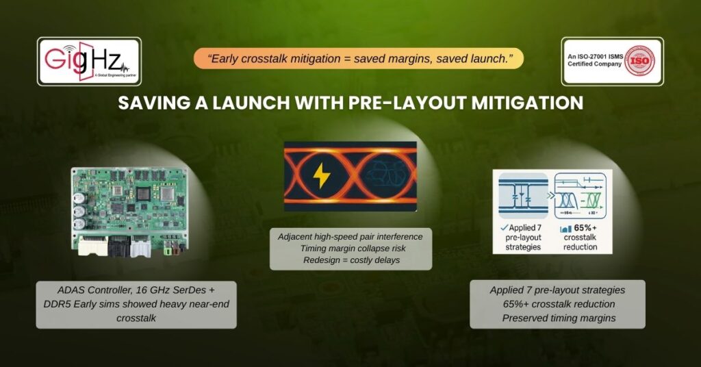
So, we were designing a multi-layer high-speed controller for an ADAS system, with multiple 16 GHz SerDes links and DDR5 running close to their limits.
Now, during our early simulations, we found significant near-end crosstalk between high-speed pairs in two adjacent layers.
Consequently, it was left unchecked, this would have meant timing failures in real-world conditions.
Besides, by applying the seven strategies below, we reduced the coupling by over 65%, preserved signal margins, and avoided a costly redesign.
7 Signal Tricks to Reduce Crosstalk in High-Speed PCB
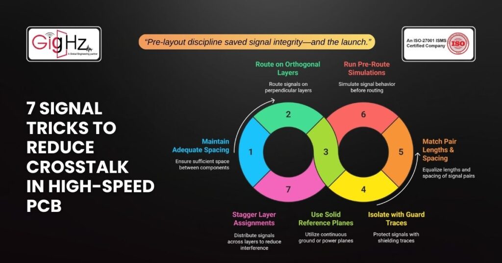
1. Maintain Adequate Spacing Early in Layout
So, for 16 GHz routing, minimum spacing rules are not completely enough. Likewise, you must go beyond IPC class recommendations and keep at least 3–4x the trace width between aggressor and victim lines to limit coupling.
2. Route on Orthogonal Layers
If you must route high-speed traces on adjacent layers, ensure they’re oriented 90° to each other. This breaks the parallel coupling path and is one of the easiest PCB crosstalk mitigation techniques you can implement without cost impact.
3. Use Solid Reference Planes
On the other hand, discontinuous ground planes are a crosstalk magnet. So, always route high-speed signals over solid, uninterrupted reference planes to provide a stable return path and minimize field fringing.
4. Isolate Critical Pairs with Guard Traces
Now, a grounded guard trace between aggressor and victim signals acts like an EMI firewall.
So, for maximum effectiveness:
- Keep guard traces continuous between driver and receiver
- Stitch to ground with vias every 1/10 of the wavelength at your highest operating frequency
5. Match Differential Pair Lengths and Spacing
Also, length-matching alone isn’t enough for spacing consistency matters just as much. So, variable spacing creates coupling “hotspots” that destroy differential signal integrity. Consequently, this is a core high-speed PCB layout trick we use on every automotive design.
6. Use Pre-Route Simulation for Crosstalk Risk Zones
Likewise, modern EDA tools let you run early-stage SI checks to flag potential high-risk coupling areas before routing is locked. So, we caught two major issues this way on our ADAS board.
7. Stagger Layer Stack Assignments
Finally, for multi-channel boards, avoid stacking multiple high-speed channels directly above each other across layers. Also, staggering assignments spread out the coupling risk across the PCB real estate.
The 24-Hour Cross-talk Check
Now, if you are stuck in the mid-design process and worried about crosstalk, then here’s the fastest win to get through it:
- Identify your top five most critical high-speed nets
- Plus, run a crosstalk simulation focused only on those nets
- Also, Apply spacing and guard trace fixes where margins are lowest
In most cases, this 24-hour check eliminates the top 80% of potential coupling problems without disrupting your design schedule.
Bottom Line
Summing up, by combining signal integrity tips for 16GHz boards with targeted PCB crosstalk mitigation, we not only saved our ADAS controller project but also passed EMI testing in the first submission.
Now, this wasn’t solely based on luck but it was the result of deliberate high-speed PCB layout tricks applied before fabrication. And the same approach works for 10 GHz, 25 GHz, and beyond.
As a final takeaway, you must:
- Space and route signals strategically
- Maintain solid reference planes
- Apply guard and ground strategies
- Validate with simulation early
Likewise, you can keep your high-speed automotive boards clean, stable, and compliant.
So, don’t let a hidden coupling path ruin your launch window. Besides, you must plan for crosstalk now—and watch your 16 GHz design sail through testing.
Accordingly, we have compiled our complete Automotive High-Speed PCB Crosstalk Prevention Guide—including simulation templates and our real-world spacing rules.
Additionally, most PCB designs fail not because of bad ideas, but because of missed checks.
So, get a free tailored improvement recommendation on your design.
As, we also offer end-to-end PCB design services to help you go from idea to final board with confidence.
Stuck in a loop of challenges? Always pick smart solution that works
Have you faced costly rework because 2D drawings skipped in MCAD workflows?
Effective way to prevent MCAD documentation errors recalls?
Please answer both poll questions before submitting.
Thank you for your response! 😊
Latest Post
Get Customized Engineering CAD Design Service

Book a Free Consultation Call
Partner with Gighz and bring your most innovative design concepts to life. Our engineering cad services accelerate development so you can focus on your big vision.