
So, you may ask this to any automotive electronics engineer about what they fear the most, and high-chances are that you will hear one word: PCB EMI Mitigation.
Ofcourse, we all get it! Now, you are someone balancing high-speed data lines, complex multi-layer routing, and dense ICs – And all of that while being scrutinized under strict automotive PCB EMI compliance standards.
Now, that’s why, when a Tier-1 automotive OEM approached us with a daunting brief of a 20-layer board, operating in a noisy under-hood environment, with non-negotiable zero EMI specs. Obviously, we knew it well that this wasn’t just about design but was majorly about control.
Likewise, we delivered the final product which passed the EMI testing on the first go itself.
So, let’s walk you through how
The Challenge: A Dense Board, No Margin for Noise
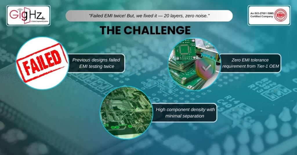
Apparently, we were tasked with building a 20-layer control unit handling ADAS-level compute, sensor fusion, and power delivery systems.
On the other hand, space constraints were brutal, and the component density was through the roof.
But here was the real kicker! They had already failed EMI testing twice with another vendor.So, what was our first step?
Well, it was to Identify exactly where their pcb emi mitigation strategy had gone off the rails.
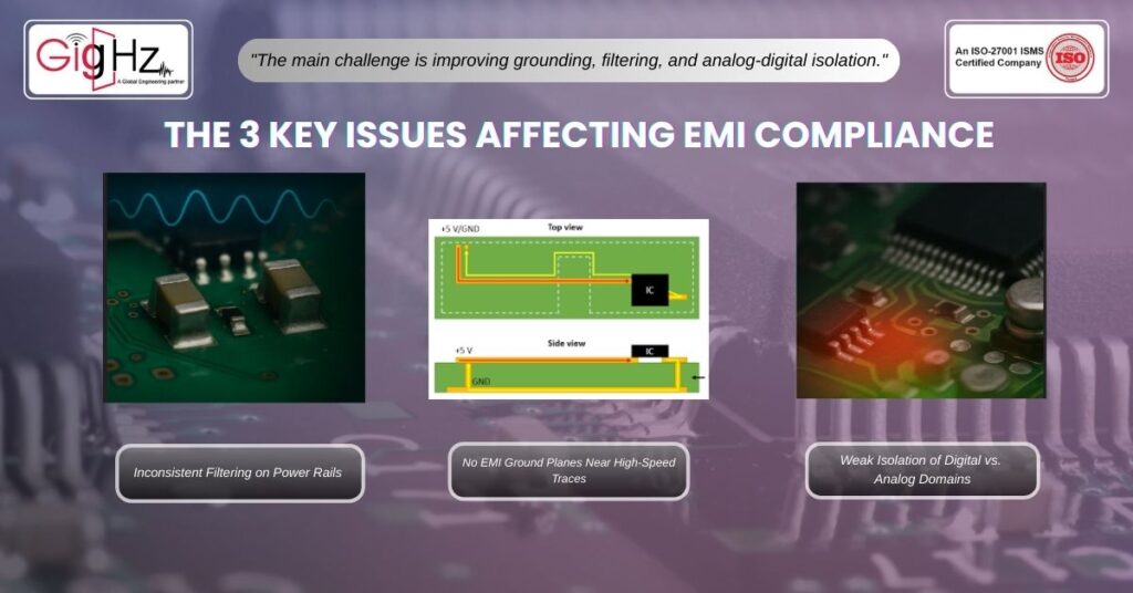
What We Found: The 3 Key Issues Affecting EMI Compliance
Evidently, even in majorly experienced design teams, it’s common to miss the subtle complexities at times.
So, here’s what we spotted in our analysis:
1. No EMI Ground Planes Near High-Speed Traces
- Firstly, without a return path close to signal layers, current loops were radiating more than necessary. Likewise, we restructured the stackup to alternate signal–ground pairs more effectively.
2. Inconsistent Filtering on Power Rails
Secondly, they had decoupling caps in place, but no uniform filtering strategy across voltage domains!
So, we brought in proven pcb emi control techniques tailored for automotive-grade noise floors.
3. Weak Isolation of Digital vs. The Analog Domains
Thirdly, the design merged with the noisy digital interfaces right next to sensitive analog sensors. So, we had to partition the PCB using local shielding and optimized zone routing.
Delayed EMI Considerations in the Flow
Finally, EMI wasn’t factored in until late in the design cycle—meaning fixes became patchwork instead of engineered solutions.
This is why we always start EMI considerations right at the stack-up planning stage, not post-layout.
It sets the foundation for a compliant design rather than forcing last-minute workarounds.
4. Areas to Improve for EMI-Safe Automotive PCB Design
Based on this project and dozens like it, here are the key practices every team should adopt:
- Begin EMI planning during stack-up definition, not after routing is done.
- Maintain continuous ground planes adjacent to all high-speed traces to minimize loop inductance.
- Apply a uniform filtering strategy across all power rails to ensure no voltage domain becomes a noise source.
- Keep digital and analog domains isolated with proper zoning and shielding techniques.
- Perform early pre-layout simulations and near-field scans instead of relying solely on compliance testing at the end.
These measures, when built into the design workflow, prevent costly re-spins and ensure the board meets automotive-grade EMI standards the first time.
The Solution: A Layer-by-Layer EMI Strategy
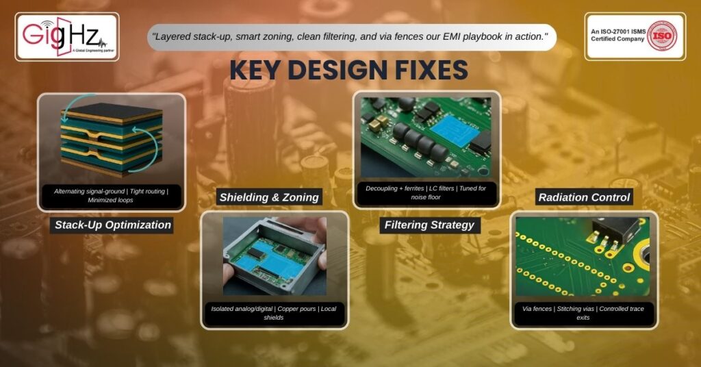
Now, here’s how we approached it:
1. Rethinking the Stack-Up
- At first, we implemented an alternating high-speed and GND layer scheme, optimized for controlled impedance. Afterwards, each differential pair had a tight return loop.
2. Shielding & Zoning
- Afterwards, we segmented the high-noise areas with the help of copper pours and strategic stitching. Also, every sensitive analog section had a clean power rail and separate plane.
3. Filter Strategy Integration
- Next, we standardized filter placements across CAN, LIN, and SPI interfaces using ferrite beads and LC filters. Consequently, this is crucial for automotive pcb emi compliance.
4. Via Fencing for Radiation Control
- Lastly, to prevent slot antenna effects, we introduced via fences around connector regions effectively lowering radiation hotspots.
The Result: A Verified Zero EMI Automotive Board
Finally, the board seamlessly passed through EMI pre-compliance and formal lab testing without a single failure. Honestly, that’s quite rare! At times, It’s even rarer for zero EMI automotive board claims to hold true in such dense environments.
But by embedding pcb emi control techniques from day one itself and not as an afterthought—we ensured a major success.
Most importantly, the majority of teams treat EMI as a post-layout checklist.
Whereas, it must begin at the stackup and partitioning level especially for automotive pcb emi compliance.
Consequently, this proactive mindset transforms EMI compliance from a last-minute hurdle into a design advantage. By integrating these practices upfront, we not only prevented costly re-spins but also accelerated the product’s path to market.
In automotive electronics, speed and reliability are everything—and EMI-safe design delivers both.
Stuck in a loop of challenges? Always pick smart solution that works
EMI challenge that keeps ruining complex PCB designs is…
The key to passing EMI tests on the first try is…
Please answer both poll questions before submitting.
Thank you for your response! 😊
Latest Post
Get Customized Engineering CAD Design Service

Book a Free Consultation Call
Partner with Gighz and bring your most innovative design concepts to life. Our engineering cad services accelerate development so you can focus on your big vision.