Common PCB Design Mistakes
As I moved forward in my career,
I quickly realized that designing with the future in mind was a critical aspect of success.
In the beginning, I often focused too much on immediate project requirements, missing the broader picture.
As a PCB designer, I’ve faced my fair share of challenges.
Whether I was working on automotive, medical, or high-speed designs, I’ve learned that even small mistakes can lead to huge headaches later on.
These lessons, learned through trial and error in my early years as a designer, have shaped the way I approach every project now.
Today, as a CEO running a company that specializes in high-quality PCB design, I often look back at those early mistakes and think about how far I’ve come.
The knowledge I gained during those initial stages of my career has been invaluable, and I now pass those lessons on to my team and clients.
Over the years, I’ve made (and corrected) some common PCB design mistakes that many engineers encounter.
If you’re just starting out or looking to refine your designs, here are the lessons I’ve learned the hard way and the fixes that helped me improve my work.
Let’s dig in!
5 Common PCB Design Mistakes I Made as a Beginner
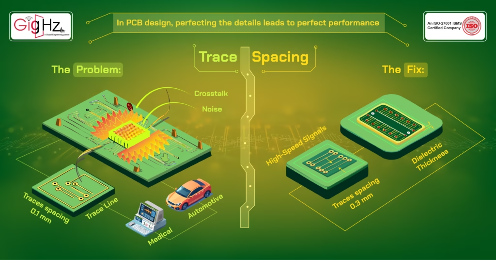
1.Trace Spacing: Giving Your Signals Room to Breathe

When I first started designing PCBs, my main focus was minimizing board size and cutting material costs.
To achieve that, I packed traces as tightly as possible, assuming that if they met the design rules, everything would work fine.
That turned out to be a big mistake.
The Problem:
I ran into issues with signal integrity, especially when working with high-speed digital circuits.
Too many traces in close proximity resulted in crosstalk and noise—especially critical in automotive and medical designs where reliability is paramount.
The Fix:
Now, as a CEO, I take a more strategic approach to design.
I make sure to give traces more breathing room.
I follow the general advice of using at least three times the dielectric thickness between traces.
With a 0.1mm dielectric, I give at least 0.3mm spacing between traces. It may seem like overkill, but it’s a game changer in terms of reducing noise and improving signal clarity.
I also route high-speed or sensitive signals away from power lines to prevent interference.
It’s a simple change, but it has saved me countless hours of debugging.
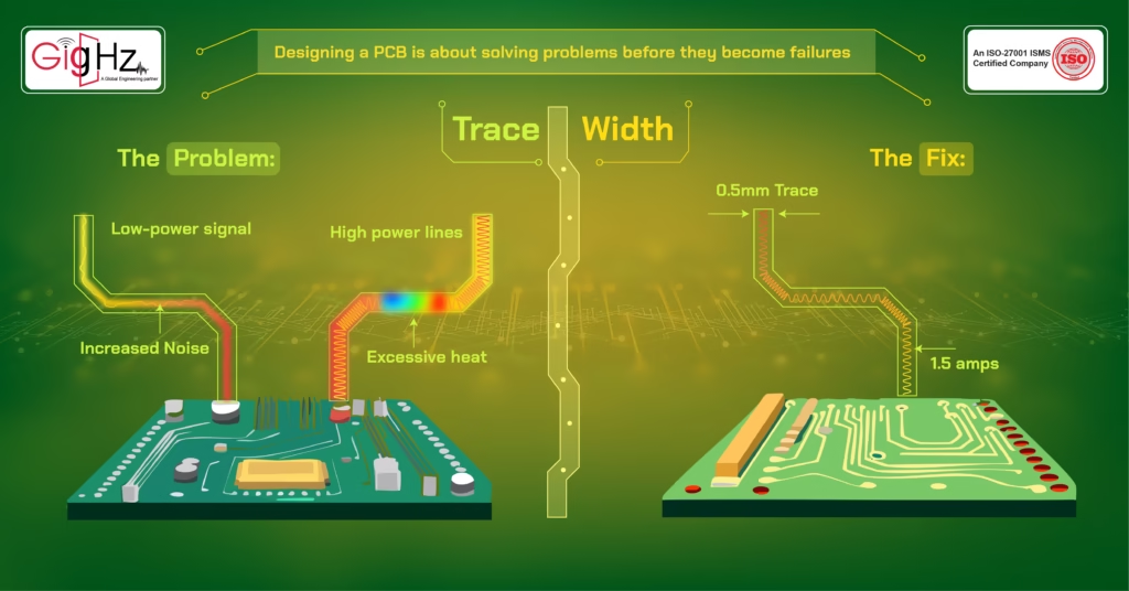
2. Trace Widths: Understanding the Right Fit for the Job

In the early days of my PCB design career, I tended to apply the same trace width for every type of signal.
I thought a wider trace was always better—after all, more metal means less resistance, right?
Unfortunately, I soon realized that wasn’t the case.
The Problem:
Using unnecessarily wide traces for low-power signals (like analog signals or data lines) resulted in increased noise susceptibility.
On the flip side, using narrow traces for high-current power lines caused voltage drops, excessive heat, and even occasional circuit failures.
The Fix:
Now, as I oversee a team of PCB designers, I emphasize the importance of tailored trace widths.
For power lines, I make sure they’re wide enough to handle the expected current. a 0.5mm trace might be suitable for 1.5 amps, but I’ve found that high-speed signal traces benefit from narrower widths—0.2mm or less, depending on the signal’s requirements.
I also use simulation tools like the Saturn PCB Toolkit to calculate precise trace widths based on current requirements. It’s a small detail, but it has a big impact on performance and reliability.
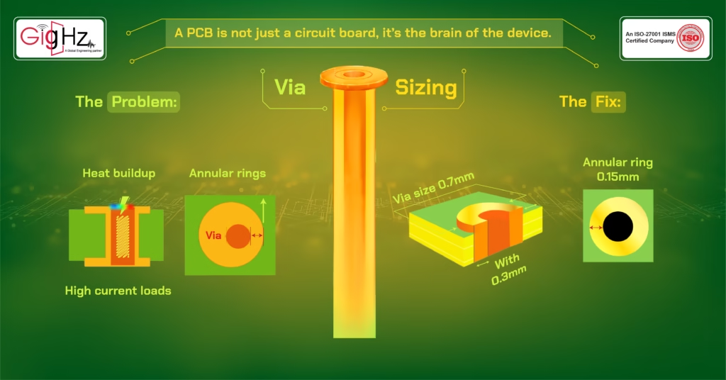
3. Via Sizing: Don’t Let Small Details Cause Big Problems

When I first got into high-density PCB designs, I was eager to save space and reduce costs, so I used smaller vias whenever possible.
I quickly learned that size does matter—especially when it comes to vias.
The Problem:
I ran into issues where my vias were too small or had inadequate annular rings.
This caused mechanical instability and sometimes failed connections.
Plus, smaller vias often had trouble handling high current loads, leading to heat buildup and reliability issues.
The Fix:
As a CEO now, I understand the importance of ensuring that every design element meets the necessary standards for performance and reliability.
I now stick to standard via sizes—0.7mm diameter with a 0.3mm drill for general applications, and I always ensure the annular ring is at least 0.15mm to ensure manufacturability and durability.
For smaller, denser designs, I’ll use microvias, but I always make sure to verify that they’re sized correctly and can handle the current they’re supposed to carry. It’s all about balance—save space where you can, but never sacrifice electrical integrity or mechanical reliability.
4. Decoupling Capacitors: Placement is Everything
I can’t count how many times I overlooked the placement of decoupling capacitors early in my career.
I would place them somewhere near the power rail, assuming they’d do their job, but the real issue was that I didn’t fully understand the importance of their proximity to the ICs.
The Problem:
In several cases, I ended up with noisy power rails, poor voltage stability, and even signal degradation. All because I wasn’t placing capacitors where they would be most effective.
The Fix:
Now, I insist on placing decoupling capacitors as close as possible to the power and ground pins of ICs, and I use a combination of different capacitor values to cover a broad range of frequencies.
A 0.1µF ceramic capacitor might filter out high-frequency noise, while a 10µF bulk capacitor handles lower-frequency fluctuations. I also keep the capacitor’s return path as short and direct as possible to minimize inductance. It’s a small detail, but it has drastically improved the power integrity and overall performance of my designs.
Final Thoughts
In the world of electronic design, understanding the common mistakes in PCB design is crucial for beginners to ensure a successful project. Many novice designers overlook the importance of a solid ground plane, which is essential for minimizing electromagnetic interference (EMI) and ensuring effective coupling between components.
Utilizing PCB design software can help create a precise schematic and PCB layout, but it’s vital to follow best practices to avoid costly errors, such as incorrect footprints or inadequate solder connections.
A thorough design review is key to identifying beginner PCB design mistakes and ensuring that elements like power supply placements and PCB trace widths are correctly implemented.
Additionally, focusing on impedance management and thermal dissipation can enhance performance. By leveraging design tools and adhering to design for manufacturing principles, designers can create the best PCB possible.
Ultimately, avoiding the 10 most common mistakes in PCB design, such as inadequate landing patterns or improper routing on the external layer, can lead to more efficient and reliable circuits.
Armed with knowledge from a PCB design review, designers will be better equipped to navigate the intricacies of EDA and create functional, robust printed circuit boards.
Want to more insights of signal integrity in pcb design?
Download our free eBook now https://gighz.net/ebook/signal-integrity/ start designing smarter today!
Latest Post
Get Customized Engineering CAD Design Service

Book a Free Consultation Call
Partner with Gighz and bring your most innovative design concepts to life. Our engineering cad services accelerate development so you can focus on your big vision.
