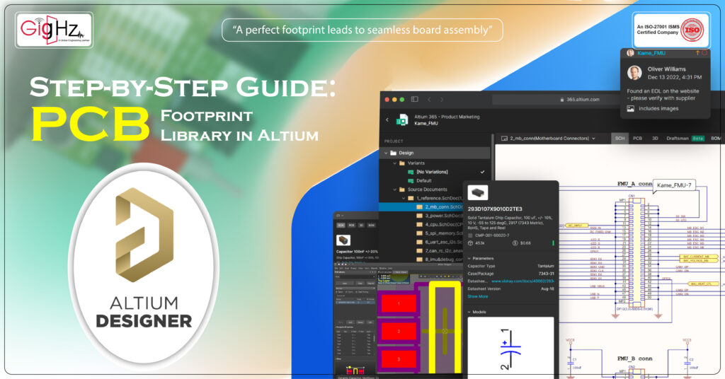
Step-by-Step Guide: PCB Footprint Library in Altium
When creating a PCB, each component should have its own distinct area in the board referred to as a PCB footprint Library. The footprint defines the component’s physical placement, including pads, holes, and outlines. An accurate footprint allows parts to fit properly, solder consistently, and the board operates correctly. Altium Designer provides tools for creating,
Step-by-Step Guide: PCB Footprint Library in Altium Read More »

